2016/05/02 (Monday)
| Setup: iZIP mode, DIB1/2/3 → cables → 3.2 MHz filters → DCRC55/33/50, DCRCs powered overnight | |
| Several temperature spikes overnight to about 58 mK | |
| 0819 | Tower/MC/Coldplate = 51.4/50.8/295 mK, Still = 0.120 mbar, G1/G2 = 107/100 mbar, 1K Pot = 1.69 K / 10.0 mbar, Main Bath = 41.0% |
| 0823 | Fill LN2 coldtraps full. |
| 0945 | Attach HV phonon rerouting board to DIB3 at the e-box. Electrical checkout on DIB3 looks good. |
|---|---|
| 0955 | Setup: HV mode, DIB1/2/3 → -/-/Phonon reroute board → cables → HV board → 3.2MHz Filters → HV1/HV2 → DCRC55/50 |
| 1033 | After zapping, Tower temp = 47.5 mK |
| 1200 | Found that phonon channel with highest Tc looked like it was in transition with 0 QET bias even though tower temp was below its Tc. Realized that Dsub filters should be placed on the fridge side of HV box to filter TESs from ac power picked up by HV box. Moved filters and zapped. |
| Setup: HV mode, DIB1/2/3 → -/-/Phonon reroute board → cables → 3.2MHz Filters → HV board → HV1/HV2 → DCRC55/50 | |
| 1330 | After zapping, was able to see pulses on HV2 PB, PC, and PD by setting rough QET biases. |
| 1445 | Performed mini-ibis on HV2. Using QET biases of HV2 PB/PC/PD = 30/15/25 uA. |
| HV2 Phonon Channel Resistances | ||
|---|---|---|
| Rnormal [Ω] | Rbiased [Ω] | |
| pB | 0.398 | 0.137 |
| pC | 0.446 | 0.121 |
| pD | 0.504 | 0.106 |
| derived from miniIbIs | ||
note the Rnormals above are a bit different from those measured on Friday.
| Attempting HV biasing using 40V power supply. Measured HV bias at power supply using multimeter. Plugging PS into variac caused “spiky” noise on PB. Turning on the variac railed PB. |
| HV bias [V] | V_leak [mV] | V_crystal [V] | PC/PD baseline [V] | Notes |
|---|---|---|---|---|
| 0 | 0 | 0 | -1.11/0.99 | |
| 1 | ~5 | -1.15(?) | -1.11/0.99 | |
| 5 | 1.5 | 4.4 | -1.11/0.99 | |
| 10 | 5→3 | 7.9→8.7 | -1.11/0.99 | Leakage current falls to ~0 within ~2 min |
| 15 | 6.5→1 | 12→15 | -1.105/0.99 | |
| 20 | 4→~0 | 18→20 | -1.1/0.995 | Pulses have flat peaks, but not at amplifier saturation level. |
| 30 | 7→1 | 27→30 | -1.08/1.02 | Lost PC pulses, PD noisy. After ~5 mins, PC starts to return, but not cleanly. |
| V_crystal = V_HV - (V_leak/1MΩ) × [430 MΩ] as determined here | ||||
| USD1 wirebonding | |
|---|---|
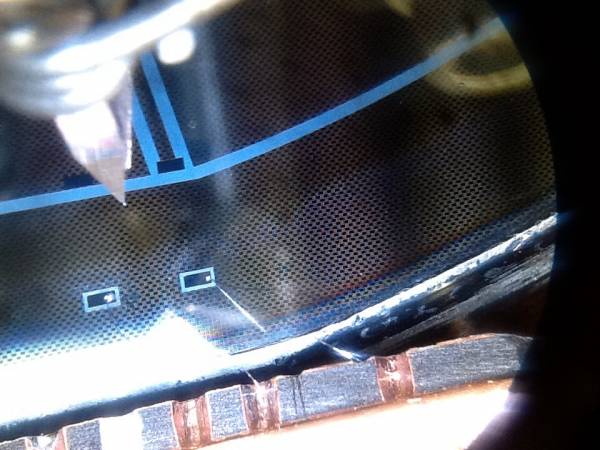
| 1015 | starting with DIB-to-detector bonds. Using bond1/bond2 set to powers 480/475, bond times 40/30, loop height 50 mils, drop before clamp 20 mils (same settings as March 31 |
| Succeeded in bonding DIB to pad for Channels 2,3,4 (numbering system is 1=outermost, 4=center). Had trouble with Channel 1, couldn't bond to pad. | |
 |
|
| Spent about 90 minutes with detector in wirebonding lab | |
| Electrical checks: found a short from Channel 2 to chassis. Removing the lid had no effect, so it was not caused by the bond touching the lid. Flipped the detector over and saw what looked like a leftover wirebond stretching down from the DIB to between DIB and detector (not sure why this should cause a short). Slid a scalpel between DIB and crystal to knock away any wirebonds. This seemed to fix the short. | |
| Electrical checks: no shorts to chassis, Channel 1 open to all other channels (of course). Interchannel resistances between 2, 3 and 4 are all 4.9 kΩ. Seems kind of high - typical interchannel resistances in most detectors are around 200 Ω. | |
| 0415 | Finally got a bond to connect from DIB to pad for Channel 1, after increasing Bond 2 power to 480. Initially this channel was showing about 180 Ω to the other channels. Then the connection to the DIB simply came loose. So I'll have to try again. About 30 minutes in the wirebonding lab. |
| 1555 | Commence LHe transfer (28.7%). |
|---|---|
| 1645 | Cease LHe transfer (92.7%). |