2016/05/03 (Tuesday)
| Setup: HV mode, DIB1/2/3 → -/-/Phonon reroute board → cables → 3.2MHz Filters → HV board → HV1/HV2 → DCRC55/50, DCRCs powered overnight | |
| Temperature basically stable overnight, started out a bit warmer then cooled to a base of 47.5 mK | |
| 0910 | Tower/MC/Coldplate = 47.7/45.8/277 mK, Still = 1.17 K / 0.110 mbar, G1/G2 = 100/100 mbar, 1K Pot = 1.65 K / 9.0 mbar, Main Bath = 63.6% |
| 0920 | Fill LN2 coldtraps full. |
| 1115 | Set up timing link between HV boards. Some high-frequency noise disappears. |
| 1130 | Set up 0-1000V power supply for HV tests. |
| Set HV to 20 V. Monitor HV2pD. Pulses look fine. Baseline unchanged. Leakage current starts at 16 nA (16 mV on test resistor), decreases to 1.5 nA after about 4 minutes | |
| Set HV to 40 V. Phonon pulses disappear. Baseline rises about 40 mV. Leakage 23→4 nA over 4 minutes. | |
| at 40 V, leakage current begins to increase. | |
| Increase HV to 50 V then back off to 40 V. Pulses return after 20 s. After 2 minutes pulses disappear again. At 3 minutes there is a temperature spike to 76 mK | |
| Reduce HV to 0, then increase to 50 V, then back off to 40 V again. No pulses. Temperature spikes corresponding with increases in leakage current. Leakage goes up then down, followed closely by temperature rise and fall. Typical current peak is 50 nA, temperature spikes from 48 mK base to 70 mK | |
| 1210 | Set HV to 30 V and leave it there a while. Over 10 minutes pulses do not return. Two temperature spikes occur, to about 58 mK. |
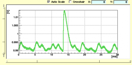
| 1225 | After turning HV back to 0, finally see pulses again, though there's a very regular low-frequency noise present on both HV2 pC & pD as seen below: |
 |
| 1240 | Noise still present. No further temperature spikes, though. Unplug DCRCs to let them “calm down.” |
|---|---|
| 1510 | Plug DCRCs back in. Zap SQUIDs. |
| 1530 | Minor low frequency noise still occasionally present, but much less significant than before. |
| 1535 | Set HV to 30V slowly and monitor temperature and pulses. Pulses still currently visible. |
| 1545 | Leakage 3.2 nA |
| 1553 | Turn up HV to 35V and pulses disappear. Leakage current: 5.1nA. No temperature response. |
| 1555 | Pulses return (though smaller than before) after ~90s. |
| 1600 | Leakage 2.1 nA |
| 1601 | Temperature spikes by 1mK. A mini-spike for some reason. |
| 1603 | Raise HV to 40V. Pulses disappear after ~30s. Leakage current: 9nA. |
| 1606 | Leakage current: 4.6nA. |
| Temperature spike to 66mK. Similar spikes happen ~90 and ~180 seconds after. | |
| 1615 | No spikes since the third one at 16:08:30. Leakage current: 4.7nA. |
| 1630 | Very soon after checking the leakage current (just like at at 16:06) after ~ 7minutes of peace, the temperature begins spiking approximately every 2 minutes. This happens for 7 spikes. Turn down the HV to 0V. Pulses return after ~60 seconds. Temperature has ceased spiking. Leakage current 11nA and dropping. |
| 1703 | Fill LN2 cold trap full. |
| 1710 | Attach Cf source to mu-metal shield at detector level. Also set up photoneutron source (strong Y source with Be target in source holder) on stool with wood blocks pointing at detector level. Intent is to activate detector overnight. |
| USD1 wirebonding | |
|---|---|
| 1600 | Repair the one broken DIB-to-detector wirebond. All 4 DIB-to-detector charge-channel wirebonds finished. |
| For detector-to-detector bonds use these settings: bond1/bond2 powers 475/475, bond times 30/30, loop height 50 mils, drop before clamp 10 mils | |
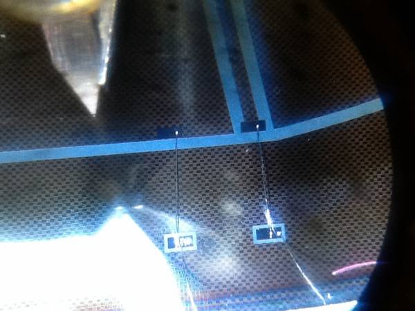
| Complete detector-to-detector bonds for charge-channel side: hopscotch connections for channels 2,3,4 and jumper connection between separate halves of channel 2 | |
 |
|
| On “phonon side” (ground side) make wirebonds from DIB1pin3 and DIB1pin5 to ground electrode. Surface seems to be uniformly covered in Al rather than a grid. | |
| Spent about 45 minutes in wirebonding lab | |
| Interestingly the resistances between channels are much smaller now that the “hopscotch” bonds are in place. Apparently the near-DIB pads are more isolated from the substrate than the channels themselves. | |
| USD1 resistance checks [Ω] | |||||||
|---|---|---|---|---|---|---|---|
| q1 | q2 | q3 | q4 | g1 | g2 | chassis | |
| q1 | - | 22.7 | 36.2 | 47.6 | 16.4 | 16.4 | open |
| q2 | - | - | 32.9 | 45.0 | 11.9 | 11.9 | open |
| q3 | - | - | - | 56.9 | 27.1 | 27.1 | open |
| q4 | - | - | - | - | 36.2 | 36.2 | open |
| g1 | - | - | - | - | - | 0.8 | open |
| g2 | - | - | - | - | - | - | open |
| resistances between four charge channels and two ground connections on opposite side |
|||||||
| USD1 pinout map | |||||
|---|---|---|---|---|---|
| q1 | q3 | q2 | q4 | g1 | g2 |
| DIB1qO | DIB1qI | DIB2qO | DIB2qI | DIB1pin3 | DIB1pin5 |
| Charge channels are numbered outer-to-inner | |||||
| A “1” is scratched onto housing above DIB1 (a little hard to see) | |||||