2016/03/31 (Thursday)
| 0900 | More on the attempt to fix G114 DIB1 pin1. |
|---|---|
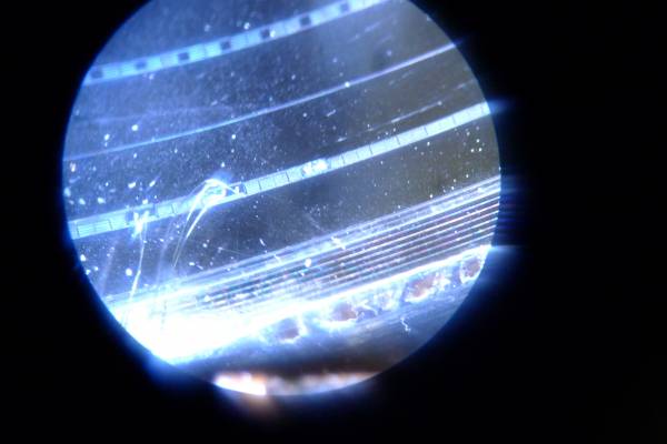
| Tried cleaning off the wirebond stubs from the pad on the detector, by gently scraping first with sharpened end of wooden swab, then (very gently) with hypodermic needle, using wirebonder microscope. Both about equally effective, some debris removed but lots remaining. Cleaned off debris by dabbing with bit of wipe dampened with isopropanol. | |
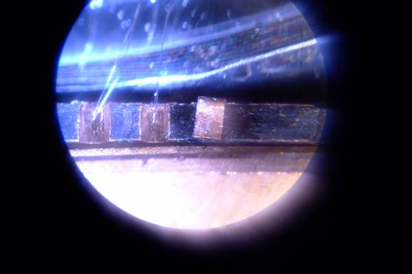
| Scraped newly made DIB bond pad with scalpel to get shiny surface | |
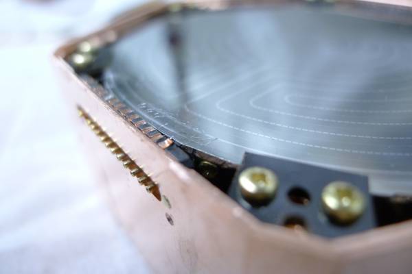
| Successfully formed two bonds from DIB to detector pad using slight variation on settings from yesterday: bond1/bond2 set to powers 480/475, bond times 40/30, loop height 50 mils, drop before clamp 20 mils | |
| Pin1-Pin2 (DIB1pA) no longer open, but rather high - about 1500 Ohm after first bond, about 1400 Ohm after second. |
| Pad on detector, after attempted cleaning | Newly made DIB pad, before scraping |
|---|---|
 |  |
| Finished wire bonds | |
 |
|
| 1115 | Take repaired G114 into clean room for electrical check. |
|---|
| Detector | G114 | DIB | 1 | |
|---|---|---|---|---|
| date/who: | 2016-03-31 | DS & AK | ||
| +lead | - lead | signal | typical | measured |
| 1 | 2 | QET A | 100 to 200 Ω | 810Ω (or 1.51 kΩ measured 2→1) |
| 3 | 4 | QET B | 100 to 200 Ω | 170.8 Ω |
| 5 | 6 | QET C | 100 to 200 Ω | 131.3 Ω |
| 7 | 8 | QET D | 100 to 200 Ω | 72.0 Ω |
| 9 | chassis | LED1 Rforward | 8 to 9 MΩ | open |
| 9 | chassis | LED1 Vforward | 1.0 to 1.1 V | open |
| chassis | 9 | LED1 Rreverse | <1 nS | <1 nS |
| 10 | chassis | LED2 Rforward | 8 to 9 MΩ | 735kΩ |
| 10 | chassis | LED2 Vforward | 1.0 to 1.1 V | 1.041V |
| chassis | 10 | LED2 Rreverse | <1 nS | <0.2nS |
| 11 | 12 | Qo-Qi | 90.4Ω | |
| 12 | 11 | Qi-Qo | 85.3Ω |
| NOTE | When measuring other channels besides DIB1 pA in reverse (i.e. pins 4→3 instead of 3→4), we measured similar readings as the forward resistances. Only with DIB1 pA was the reverse value drastically different. |
|---|
| Detector | G114 | DIB | 2 | |
|---|---|---|---|---|
| date/who: | 2016-03-31 | DS & AK | ||
| +lead | - lead | signal | typical | measured |
| 1 | 2 | QET A | 100 to 200 Ω | 159.7 Ω |
| 3 | 4 | QET B | 100 to 200 Ω | 35.4 Ω |
| 5 | 6 | QET C | 100 to 200 Ω | open (<0.2nS) |
| 7 | 8 | QET D | 100 to 200 Ω | 35.2 Ω |
| 9 | chassis | LED1 Rforward | 8 to 9 MΩ | 733kΩ |
| 9 | chassis | LED1 Vforward | 1.0 to 1.1 V | 1.040V |
| chassis | 9 | LED1 Rreverse | <1 nS | <0.5nS |
| 10 | chassis | LED2 Rforward | 8 to 9 MΩ | 735 kΩ |
| 10 | chassis | LED2 Vforward | 1.0 to 1.1 V | 1.042V |
| chassis | 10 | LED2 Rreverse | <1 nS | <0.5nS |
| 11 | 12 | Qo-Qi | 396kΩ | |
| 12 | 11 | Qi-Qo | 1.2 ± 0.2MΩ |
| NOTE | Pin 5 is connected to all other phonon channels, whereas Pin 6 is open to all other phonon channels. Pin 6 is the pin that's disconnected now. |
|---|
| Detector | G114 | DIB | 3 | |
|---|---|---|---|---|
| date/who: | 2016-03-31 | DS & AK | ||
| +lead | - lead | signal | typical | measured |
| 1 | 2 | QET A | 100 to 200 Ω | open |
| 3 | 4 | QET B | 100 to 200 Ω | 84.7 Ω |
| 5 | 6 | QET C | 100 to 200 Ω | 30.7 Ω |
| 7 | 8 | QET D | 100 to 200 Ω | 83.3 Ω |
| 9 | chassis | LED1 Rforward | 8 to 9 MΩ | open |
| 9 | chassis | LED1 Vforward | 1.0 to 1.1 V | |
| chassis | 9 | LED1 Rreverse | <1 nS | |
| 10 | chassis | LED2 Rforward | 8 to 9 MΩ | open |
| 10 | chassis | LED2 Vforward | 1.0 to 1.1 V | |
| chassis | 10 | LED2 Rreverse | <1 nS | |
| 11 | 12 | Qo-Qi | open | |
| 12 | 11 | Qi-Qo | open |
| NOTE | Neither pins 1 or 2 showed connections to any of the other phonon channels, suggesting that both pins 1 & 2 are disconnected now. |
|---|
| 1200 | After examining the wirebonds visually, we saw several “hanging” wirebonds on DIB3 (i.e. only attached on the DIB pads). It appeared that all four wirebonds that connect DIB3 pins 1&2 were affected. DIB2 pin6 was less visually affected, but it's most likely a similar diagnosis. |
|---|---|
| Reattach cover of G114 and replace in anteroom for more wirebonding. | |
| 1205 | Remove tower from purge cabinet and remove copper plate from bottom of Side 6 to examine missing socket. It appears that the sockets are simply soldered to a pad at the bottom of the tower. The fear is that the pad may have come off completely. |
| 1235 | The pad has come off, though there's a small dot where the wire from the tower face comes through the PCB and connects to where the pad/socket should be. |
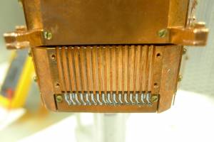
| Tower face with plate removed. There's a wire running through each channel. | Missing socket | Missing socket |
|---|---|---|
 | 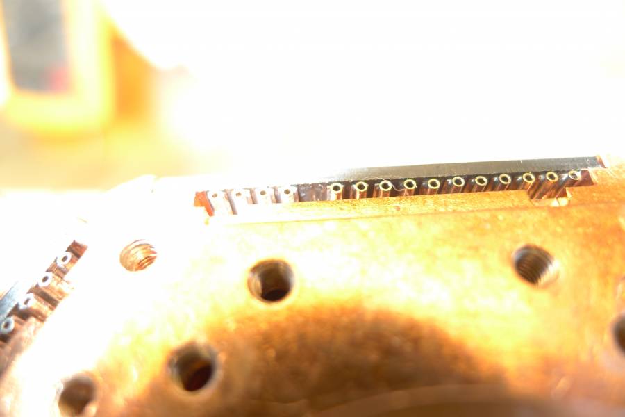 | 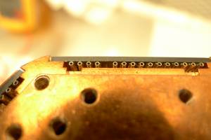 |
| Screws removed from the connector board of one of the “bad” faces. The board hinges out somewhat under the tension of the wires. | Screws removed from the connector board on the face with the missing socket. | |
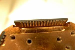 | 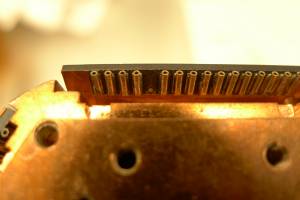 |
There's no clear way to fix this.
| 1235 | Perhaps some of the other “bad” tower faces are more easily fixable. Test through-connections of each Tower Face. |
|---|
| Tower Face | Good Trace Resistances | Open Traces | Shorted To Ground | Shorts from One Pin to Another |
|---|---|---|---|---|
| Face 4 | ~27Ω | none | none | none?!?! |
| Face 5 | ~27Ω | none |
| 1500 | Repaired DIB-to-detector connections for DIB2 pin6 and DIB3 pins 1&2 with the wirebonder. Scraped DIB pads gently with scalpel or hypodermic needle in direction along the trough. |
|---|
| 1550 | Back in the clean room after a long afternoon of run-diary investigations to determine what had caused the labelling of “Bad” for Tower Faces 1,3,4. In the run diary all that is said is that after using Tower Face 4 in Run 4, the tower level electrical check for Run 5 said: |
|---|
- One connector found to have a damaged pin.
- One connector gave strange results when an electrical check was performed.
- Both sides have been labelled so as not to be used again.
| No other information is given in any of the surrounding daily run-diary pages. The official electrical checkout for Run 5 only lists Tower Face 5, which was finally used after the two anonymous faces were deemed bad (we suspect Tower Faces 3&4. According to an eLog entry Tower Face 1 was already bad when it was sent to us. |
| In the clean room begin examining face 3 because if that's actually good, we could run using Faces 2,3,5. |
| Tower Face | Good Trace Resistances | Open Traces | Shorted To Ground | Shorts from One Pin to Another |
|---|---|---|---|---|
| Face 3 | ~28Ω | none | Loose Socket 15, which could short to ground or other pins. Socket 1 shorts to the 4K stage, but not 600mK ears. | Potentially Socket 15 |
| Face 1 | ~29Ω | Socket 5,6,7,8,9,10 | Did Not Bother | Did Not Bother |
| 1620 | Repaired G114 is back in clean room. Perform detector level electrical checkout: |
|---|
| Detector | G114 | DIB | 1 | |
|---|---|---|---|---|
| date/who: | 2016-03-31 | DS & AK | ||
| +lead | - lead | signal | typical | measured |
| 1 | 2 | QET A | 100 to 200 Ω | 809Ω (or 1.6 kΩ measured 2→1) |
| 3 | 4 | QET B | 100 to 200 Ω | 171.0 Ω |
| 5 | 6 | QET C | 100 to 200 Ω | 131.3 Ω |
| 7 | 8 | QET D | 100 to 200 Ω | 72.0 Ω |
| 9 | chassis | LED1 Rforward | 8 to 9 MΩ | open |
| 9 | chassis | LED1 Vforward | 1.0 to 1.1 V | open |
| chassis | 9 | LED1 Rreverse | <1 nS | <1 nS |
| 10 | chassis | LED2 Rforward | 8 to 9 MΩ | 742kΩ |
| 10 | chassis | LED2 Vforward | 1.0 to 1.1 V | 1.042V |
| chassis | 10 | LED2 Rreverse | <1 nS | <0.2nS |
| 11 | 12 | Qo-Qi | 90.7Ω | |
| 12 | 11 | Qi-Qo | 85.8Ω |
| Detector | G114 | DIB | 2 | |
|---|---|---|---|---|
| date/who: | 2016-03-31 | DS & AK | ||
| +lead | - lead | signal | typical | measured |
| 1 | 2 | QET A | 100 to 200 Ω | 158.0 Ω |
| 3 | 4 | QET B | 100 to 200 Ω | 35.4 Ω |
| 5 | 6 | QET C | 100 to 200 Ω | 108.7 Ω (backwards reading 6→5 read similar value) |
| 7 | 8 | QET D | 100 to 200 Ω | 35.3 Ω |
| 9 | chassis | LED1 Rforward | 8 to 9 MΩ | 740kΩ |
| 9 | chassis | LED1 Vforward | 1.0 to 1.1 V | 1.042V |
| chassis | 9 | LED1 Rreverse | <1 nS | <0.3nS |
| 10 | chassis | LED2 Rforward | 8 to 9 MΩ | 742 kΩ |
| 10 | chassis | LED2 Vforward | 1.0 to 1.1 V | 1.043V |
| chassis | 10 | LED2 Rreverse | <1 nS | <0.3nS |
| 11 | 12 | Qo-Qi | 484kΩ | |
| 12 | 11 | Qi-Qo | 1.15 ± 0.1MΩ |
| Detector | G114 | DIB | 3 | |
|---|---|---|---|---|
| date/who: | 2016-03-31 | DS & AK | ||
| +lead | - lead | signal | typical | measured |
| 1 | 2 | QET A | 100 to 200 Ω | 31.2 Ω (reverse reading 2→1 gives similar result) |
| 3 | 4 | QET B | 100 to 200 Ω | 84.6 Ω |
| 5 | 6 | QET C | 100 to 200 Ω | 30.9 Ω |
| 7 | 8 | QET D | 100 to 200 Ω | 83.5 Ω |
| 9 | chassis | LED1 Rforward | 8 to 9 MΩ | open |
| 9 | chassis | LED1 Vforward | 1.0 to 1.1 V | |
| chassis | 9 | LED1 Rreverse | <1 nS | |
| 10 | chassis | LED2 Rforward | 8 to 9 MΩ | open |
| 10 | chassis | LED2 Vforward | 1.0 to 1.1 V | |
| chassis | 10 | LED2 Rreverse | <1 nS | |
| 11 | 12 | Qo-Qi | open | |
| 12 | 11 | Qi-Qo | open |
| 1625 | All the broken channels are fixed. DIB1 pA is still showing high resistance, but most likely within runnable range. |
|---|---|
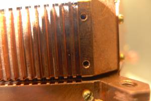
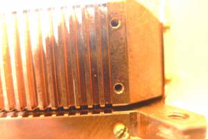
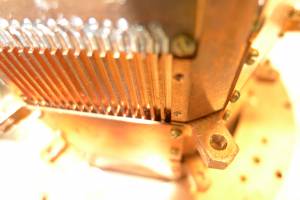
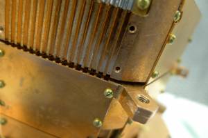
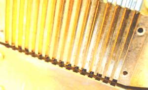
| 1630 | Back to Tower Face 3, take off the lowest copper plate and investigate to see why Socket 1 is shorted to the 4K Stage ground. It looks like the wire –unlike its brethren – is slanted in its vacuum channel and contacts the copper sidewall (see below). This is most likely the culprit of the short to ground. |
| Tower Face 3 Vacuum Channel Wires with 4K Stage Face-Plate Removed | |
|---|---|
| Channel 1 is on the right | Brightened/Increased Contrast Image |
 |  |
 |
|
| Original: Notice How Channel 1's Wire Disappears To The Left As It Descends | Brightened/Increased Contrast Image |
 |  |