Previous Day
| 1000 | Spent about 4 hours trying to wirebond G114 DIB1 pin1 DIB to detector. |
| | Finally got a bond to connect from DIB pad to detector pad, with power settings 475/450 for bond1/bond2 (DIB/detector), with drop-before-clamp setting of 24 (because detector is significantly lower than DIB pad), and with a large horizontal overshoot past the detector pad before lowering the bonder tip to connect with the detector pad. |
| | However, pin1 still read open to other pins. It turns out that in preparing the DIB pad copper surface by scraping it I wound up disconnecting the DIB pad from the vertical DIB trace. |
| | Another potential problem is that I've made a mess of the pad on the detector with multiple bond attempts. I may have created a short. |
| Photos through wire bonder microscope |
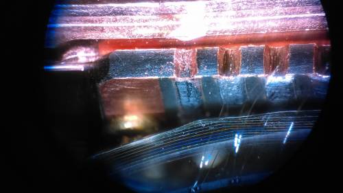 | 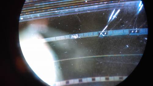 |
| Damaged DIB pad | Pad on detector covered with wirebond stubs |
| Possibility of short |
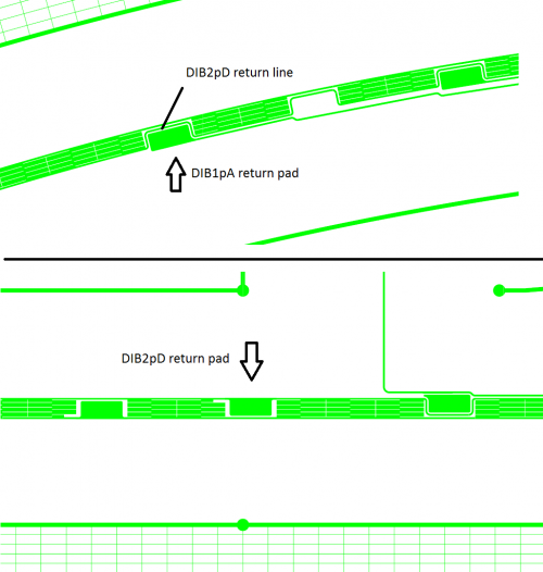 |
Examining the mask diagram for iZIPv6 and the detector pad photo above, it looks like if a short was created by the wirebond stub mess, most likely it is between the returns of DIB1pA (Side1pB) and DIB2pD (Side1pA, the outer channel). Since these both feed directly to ground at the DCRC, this is luckily not too bad. It will create a ground loop, but it shouldn't leak bias current from one channel to another. There's also a smaller chance of a short across DIB2pD (Side1pA) which would of course make it impossible to bias that phonon channel.
Followup: After fixing the G114 connections, checked the resistance between DIB1 pin1 and DIB2 pin3 (the two I thought might be shorted), as well as several other cross-DIB resistances. No evidence of a short. Actually all DIB1 pin1 to other pin resistances seemed to be around 800 Ω. Still not sure why there is such a high resistance on this connection.
| 1400 | Tried to connect the DIB pad to the vertical trace with a little solder, made another mess… in the end wound up completely removing copper from DIB pad. |
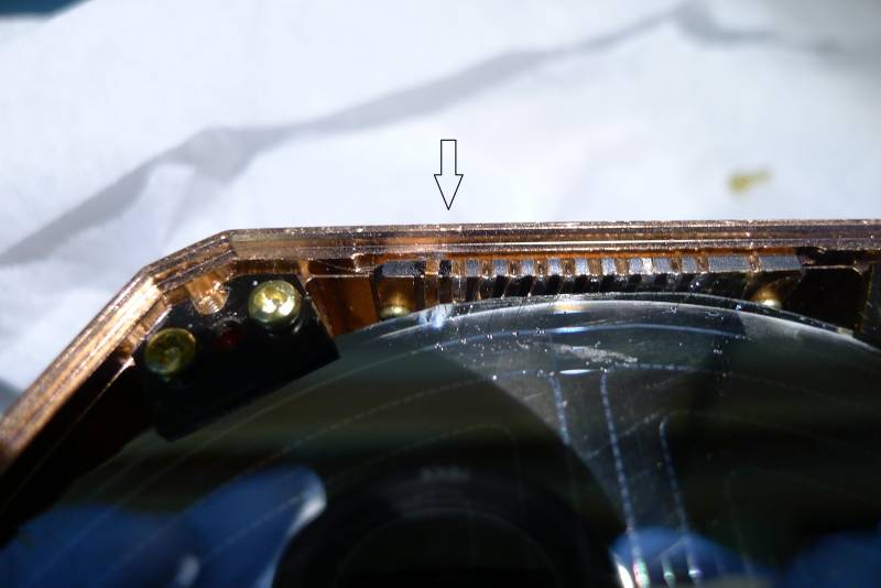
| 1700 | Attempted to repair DIB1 pin1 pad-to-trace continuity with L-shaped piece of copper foil about 1mm wide, long side soldered to vertical trace with short side forming bond pad at top. |
| | Checked continuity from pin1 to DIB pad: OK. Rechecked continuity from pin2 to others: OK. Checked lack of continuity of pin1 and pin2 to chassis: OK. |
Next Day