To study the source of HV noise, the noise was examined while applying HV bias to subsets of the side 2 phonon channels. Custom Dsub switchboards were inserted at the ebox to short the appropriate bias connections.
The data was taken on 20171220.
When the HV bias is applied, all channels exhibit a rise in phonon baseline levels. This is because some source of parasitic power is heating the TESs, pushing them further up the transition. The amount of parasitic power can be calculated using the calculated dp/di values. The figure below shows how this implied parasitic power level on each channel changes under different bias conditions. The x-axis is channel number with 0-5 corresponding to A-F, the y-axis is the change in baseline from 0 V to 70 V bias converted from output voltage to power at the TES. The 4 scenarios represented are; standard setup (bias all side 2 channels), switchboard inserted on DIB3 but still bias all channels, switchboard inserted on DIB3 and S2PA not biased, switchboards inserted on all 3 DIBs and only bias S2PA.
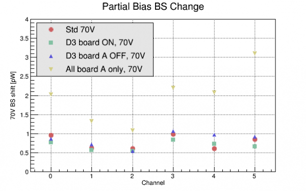
It is clear that adding the switchboard and not biasing PA does not add significant parasitic power. However, HV biasing with only PA roughly doubles the total parasitic power seen by the side 1 channels. Biasing to the same potential with only PA requires a higher charge density and results in larger peak fields near the electrode which is correlated with higher leakage.
Previous studies have indicated that the HV noise is shot noise from a small current of carriers traversing the crystal. This should result in a rise in the psd that flattens out at frequencies below the pulse fall time. As seen shown in the figure below, there is a rise, but it doesn't seem to flatten out.
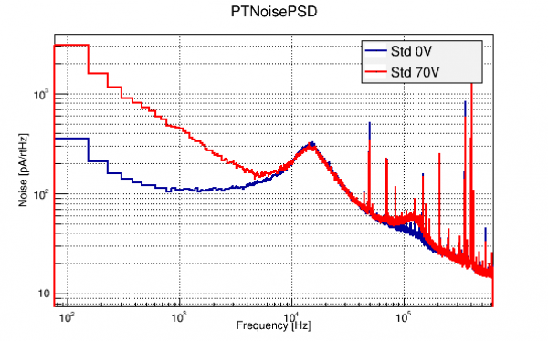 | 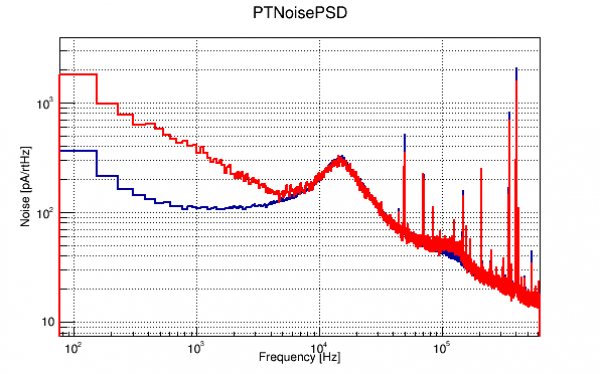 |
| Calculated using BatNoise | + flatBScuts |
The difference of the 0V and HV psds should show the excess noise due to HV biasing. This is shown in the figure below for the same scenarios described above.
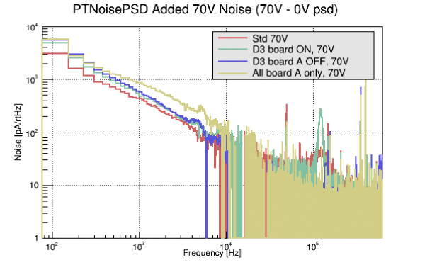 | 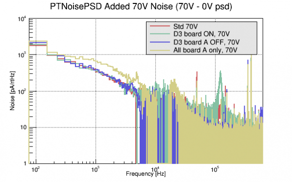 |
| Calculated using BatNoise | + flatBScuts |
One possible issue was that the PSDs include only rudimentary pulse cuts and have no flat baseline requirement. This may allow long muon tails to enhance the low frequency components of the psds. A feature was added to BatNoise to allow one to impose cuts on the PT baseline slope. This indeed resulted in a decrease of the low frequency noise components.
All scenarios again show leakage with HV with the PA only biasing having the most. The excess psd noise can be converted to a power noise as described here and here. However, using the second lowest frequency bin in the psds above as a conservative estimate of the DC noise level (the lowest bin is suspect because DFFT is weird), and folding in estimates of the phonon collection efficiency and dPdI, one obtains an ~4pA leakage current which corresponds to ~14pW parasitic power load on the TESs. This an order of magnitude larger than the parasitic power calculated from baseline shifts above. Running the calculation the other direction indicates that the observed baseline shift should correspond to an excess 0-frequency psd level of ~250 pA/rtHz at 70V.