S101 (HV#4) was wirebonded following a scheme from Noah that would allow all 12 phonon channels to be read out.
This is the scheme:
| Noah's 12-channel wirebonding scheme | ||||
|---|---|---|---|---|
| pA | pB | pC | pD | |
| DIB1 | TES4 | tes10 | tes9 | TES2 |
| DIB3 | tes11 | tes8(d4) | TES5 | TES3(d1) |
| DIB4 | tes7 | tes6 | TES1 | TES0 |
| CAPITALS = Side1, lowercase = Side2 | ||||
| (d4) and (d1) refer to the DIBs that these channels' bond pads are located near. Noah's scheme extends wirebonds past the standard pad positions into these two B-ring channels |
||||
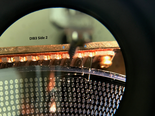
tes8 was actually left unbonded by Matt Cherry because it would conflict with the TES11 bonds. It was agreed that the TES11 and TES8 connections could be swapped - this was left for UMN to do. The detector can't be run in HV (with side1 readout) as is because tes8 can't be biased. So some extra bonding is necessary. (Update: see below. It seems that TES3 was also left unbonded, and suggested that TES3 and TES5 could be swapped similarly.)
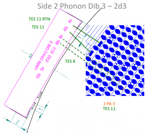 |  |
Noah's scheme does not match our HV board wiring. Not only are the particular channel assignments within a DIB a mismatch, but worse, the number of Side1 channels per DIB is a mismatch. The HV board is wired such that the channels from one side are arranged in a 3/2/1 pattern across the three DIBs. But Noah's scheme has them in a 2/2/2 pattern. To connect this properly to the HV board would require jumpers extending from one of our rerouting boards to another. Matt F, Noah, and Nick M are all in agreement that this needs to be avoided, it would be too noisy (and mechanically inconvenient).
For reference here is the basic wiring layout of the HV board:
| HV board wiring layout | ||||
|---|---|---|---|---|
| pA | pB | pC | pD | |
| DIB i | SIDE X | SIDE X | SIDE X | side y |
| DIB ii | side y | side y | SIDE X | side y |
| DIB iii | side y | side y | SIDE X | SIDE X |
| The particulars of which DIB and which Side are not important, so they are labeled here generically |
||||
There are various solutions for matching to the board, for example:
- Switch tes11 wirebond on DIB3 from pA to pB and bond tes8 to pA
- Remove tes10 bonds from DIB1pB and short tes10 to tes9
- Remove TES3 bonds from DIB3pD and connect them to DIB1pB
| Solution 1 scheme | ||||
|---|---|---|---|---|
| pA | pB | pC | pD | |
| DIB1 | TES4 | TES3 | tes9(-tes10) | TES2 |
| DIB3 | tes8(d4) | tes11 | TES5 | n/c |
| DIB4 | tes7 | tes6 | TES1 | TES0 |
This would sacrifice tes10 (which is an inner-ring Side 2 channel) and would require a rerouting board for DIB1 to swap pC and pD. As an alternative we could try to swap these two channels in the wirebonding, then we wouldn't need a rerouting board.
Noah has suggested that it if we were going to sacrifice channels it would be best if they were A-ring (outer ring) channels. However this may not be possible.
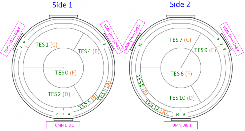 |
| G101c SNOLAB HV prototype channel layout. Also shown are the positions of the bond pads near each DIB. Two DIBs are thinner than standard because they are not at the detector flats. |
|---|
December 16 email from Matt Cherry:
S101 will arrive Monday, barring weather.
Sorry I did not send it sooner.  I was nursing it while trying to sort out a few lingering issues, and was attempting decipher the
DIB3 issue mentioned below without removing the bonds that were already in place.  I made no progress.  Those two channels might
not be recoverable.
It is bonded according to the previously attached scheme, with 2 caveats: neither of the "jumper" channels are feasible.  In both
cases (one per side) there is another set of wires that pass in front of the intended DIB pads.  If Matt F. wants, he can swap the
wiring to accommodate, but I'd suggest running as-is first.  To isolate the QETs for bonding, simply use a tip with no wire in it,
(preferably a dirty one, as it won't be usable afterward).  If the bonding "trigger height" is set slightly below the surface, and
the force and ultrasonic settings are high, the tip will destroy the metals underneath.  There are small spurs leading to each
side of the QET that can be cut for this purpose.  As the fins are not connected, its usually best to try and bridge a couple fins
with the bond foot to give yourself more connected aluminum to work with.
comment: This technique of using the wirebonder tip to perform surgery (destroy metal connections) on the detector surface is probably not something I can do with our shared wirebonder. I don't know of an extra “dirty” tip, or whether those nominally in charge of the wirebonder would approve of using the machine this way. Are there alternatives? Does a scalpel work?
In addition, there are 3 problems.
1 & 2) DIB3 has two channels bonded, one per side.  Ch. A is reading as 1.55Mohm, while Ch. C is reading as open, despite being
connected.  I'm not sure if this is a problem with the DIB or with my bonding jumper strategy (which worked elsewhere).  I suspect
the DIB...
comment: Two open or nearly open channels. If the DIB is at fault we can check DIB continuity after removing the wirebonds from DIB to detector, or possibly even before.
3) There are only LEDs on the "thick" DIB, DIB2.  Again, one per side.  Unfortunately, the LED attached to PIN9 might be bad.
This is on side 1.  It is not reading correctly, measuring ~4Mohm and ~.3nS.  PIN10 measures the nominal ~9.8Mohm and 0.04nS.
comment: Only one LED sounds like a problem. Should we use our external LEDs? This will probably be difficult since we also want to use an internal source. Of course we still don't know what the internal source will be…
Aside from that, here are the remainder of the channel resistances, in ohms.
DIB1:
	A = 342.2
	B = 411.0
	C = 339.9
	D = 369.6
DIB2:
	A = 296.3
	B = 350.9
	C = 287.3
	D = 387.1
Matt [Cherry]
| what Matt Cherry sent | ||||
|---|---|---|---|---|
| pA | pB | pC | pD | |
| DIB1 | TES4 | tes10 | tes9 | TES2 |
| DIB3 | tes11 (R very high) | n/c | TES5 (open) | n/c |
| DIB4 | tes7 | tes6 | TES1 | TES0 |
| tes8 and TES3 not connected | ||||
Suppose we want to go with Solution 1+ (that's solution 1 but with the extra channel swap to fully accommodate the HV board:
| Solution 1+ scheme | ||||
|---|---|---|---|---|
| pA | pB | pC | pD | |
| DIB1 | TES4 | TES3 | TES2 | tes9(-tes10) |
| DIB3 | tes8(d4) | tes11 | TES5 | n/c |
| DIB4 | tes7 | tes6 | TES1 | TES0 |
It would require the following steps:
| 1 | side1 | dib1 | pB | bond to TES3 (long bonds) |
| 2 | side1 | dib1 | pD | remove bonds to TES2 |
| 3 | side1 | dib1 | pC | bond to TES2 (long bonds) |
| 4 | side1 | dib3 | pC | redo pin6 bond to TES5 |
| 5 | side2 | dib1 | pB | remove bonds to tes10 |
| 6 | side2 | dib1 | pC | remove bonds to tes9 |
| 7 | side2 | dib1 | pD | bond to tes9 and jump tes10 to tes9 |
| 8 | side2 | dib3 | pA | remove bonds to tes11 |
| 9 | side2 | dib3 | pA | bond to tes8, which requires surgery |
| 10 | side2 | dib3 | pB | bond to tes11 |
We would have to see whether the outer ring channels, which are currently reading high or open, are improved by the above: step 4, redoing the connection on TES5 that seems open, and step 10, connecting tes11 to a different DIB channel.