2017/02/22 (Wednesdei)
| Setup: DIB1/3/4 → 3.2 MHz filters 3/1/2 → cable 3/1/2 →gender changer 3/1/2 → HVConn 1/3/2 → HV 1/2 → DCRC55(1)/DCRC33(2) | |
| 0915 | Tower/MC/Coldplate = 33.7/30.9/197 mK, Still = 1.30 K / 0.110 mbar, G1/G2 = 231/228 mbar, 1K Pot = 1.673 K / 22 mbar, Main bath = 67.2%. Boil off rate: a bit faster than slow mode. |
| 0920 | Fill LN2 cold trap bath |
| 0949 | Modify side2 HV board to remove bias from Conn2 charge lines. This was the only connector on which the charge related lines were biased. Conn3 was left open on the board and Conn1 goes straight through to the DCRC. This connector corresponds to DIB4 in the current setup, which had shown some charge-related shorts to ground in electrical checks. |
| 0955 | A quick break-out box check on DIB4 shows 20 nS from QI Fb→Gnd, 9 MΩ from gnd→Qi source/Drain. These are consistent with a ~9 MΩ a short to ground somewhere between the coupling capacitor, feedback resistor, and the FET gate. In addition, performing this measurement heats the tower ~3 mK |
| 1001 | Set up in HV side 2 mode again with modified HV board. Setup: DIB1/3/4 → 3.2 MHz filters 3/1/2 → cable 3/1/2 →gender changer 3/1/2 → HVConn 1/3/2 → HV 1/2 → DCRC55/DCRC33 |
| 1005 | Power on DCRCs, tower temp spikes to 294 mK |
| 1024 | Tower temp back at 35 mK. Start DCRC programs and zap SQUIDs. |
| 1044 | Pulses seen on both DCRCs. Apply HV to detector using the 0-1 kV Kepco power supply. Increase voltage and check leakage across test resistor. At each voltage, measure leakage again after a couple minutes. Also record the baseline of the DCRC1pB trace. It seems to be less noisy than DCRC1 PA which was used before. DCRC1 PB FE Gain/Driver Gain/QET Bias = 20/1/151.76 |
| HV [V] | Vtest [mV] | Ileak [nA] | Vcrystal [V] | DCRC1pB baseline [V] |
|---|---|---|---|---|
| 0 | 0 | 0 | 0 | -0.0466 |
| 2 | 2.1 | 2.31 | 1.08 | -0.0469 |
| 2 | 0.7 | 0.77 | 1.69 | -0.0466 |
| 5 | 3 | 3.3 | 3.68 | -0.0469 |
| 5 | 1 | 1.1 | 4.56 | -0.0473 |
| 10 | 8.3 | 9.13 | 6.35 | -0.047 |
| 10 | 1.6 | 1.76 | 9.3 | -0.0464 |
| 15 | 5.5 | 6.05 | 12.58 | -0.0471 |
| 15 | 1.4 | 1.54 | 14.38 | -0.0471 |
| 20 | 1.3 | 1.43 | 19.43 | -0.0459 |
| 20 | 1.8 | 1.98 | 19.21 | -0.0459 |
| 20 | 0.3 | 0.33 | 19.87 | -0.0462 |
| 30 | 12.1 | 13.31 | 24.68 | -0.046 |
| 30 | 2.9 | 3.19 | 28.72 | -0.0448 |
| 30 | 2 | 2.2 | 29.12 | -0.0453 |
| 40 | 10.3 | 11.33 | 35.47 | -0.0449 |
| 40 | 2.4 | 2.64 | 38.94 | -0.045 |
| 40 | 1.3 | 1.43 | 39.43 | -0.0447 |
| 50 | 14 | 15.4 | 43.84 | -0.0443 |
| 50 | 4.1 | 4.51 | 48.2 | -0.0448 |
| 50 | 3.9 | 4.29 | 48.28 | -0.0441 |
| 50 | 3.1 | 3.41 | 48.64 | -0.0433 |
| 60 | 8.8 | 9.68 | 56.13 | -0.0423 |
| 60 | 4 | 4.4 | 58.24 | -0.0414 |
| 70 | 6.4 | 7.04 | 67.18 | -0.0406 |
| 70 | 5 | 5.5 | 67.8 | -0.041 |
| 80 | 14.3 | 15.73 | 73.71 | -0.0394 |
| 80 | 3.4 | 3.74 | 78.5 | -0.0387 |
| 90 | 19.6 | 21.56 | 81.38 | -0.0375 |
| 90 | 10.3 | 11.33 | 85.47 | -0.0398 |
| 90 | 8.5 | 9.35 | 86.26 | -0.0387 |
| 100 | 13.4 | 14.74 | 94.1 | -0.0384 |
| 100 | 9 | 9.9 | 96.04 | -0.0407 |
| 100 | 5.5 | 6.05 | 97.58 | -0.0391 |
formulas:
- Ileak [nA] = 1.1 * Vtest [mV]
- Vcrystal [V] = HV [V] - 0.4 * Ileak [nA]
| 1223 | Complete positive voltage scan. Base temperature remained stable at 39 mK and pulses looked clean throughout entire scan. |
|---|---|
| 1225 | Reduce voltage to 80V |
| HV [V] | Vtest [mV] | Ileak [nA] | Vcrystal [V] | DCRC1pB baseline [V] |
|---|---|---|---|---|
| 80 | -1.7 | -1.87 | 80.75 | -0.0377 |
| 80 | 3.2 | 3.52 | 78.59 | -0.406 |
| 80 | 5.1 | 5.61 | 77.76 | -0.0416 |
| 1254 | Re measure values after waiting 20 mins |
|---|
| HV [V] | Vtest [mV] | Ileak [nA] | Vcrystal [V] | DCRC1pB baseline [V] |
|---|---|---|---|---|
| 80 | 5.6 | 6.16 | 77.54 | -0.0413 |
| 1255 | Turn HV back to 0V. |
|---|---|
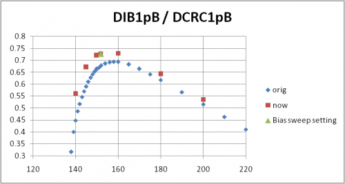
| 1329 | Perform mini IbIs on DCRC1 PB. It looks like we were rather high in the transition during this sweep. A lower setting would have given a more sensitive baseline. |
| 1350 | Inspecting and installing spare 1“ DIBs on 150mm, 1” housing in preparation to send to A&M. |
|---|
| DIB number | 53 | ||
|---|---|---|---|
| +lead | - lead | signal | measured |
| 1-8,11-12 | chassis | Phonons/Charge | <0.2 nS |
| 9 | chassis | LED1 | 0.774 MΩ |
| 9 | chassis | LED1 | 1.055 V |
| chassis | 9 | LED1 | 0.3 nS |
| 10 | chassis | LED2 | 0.752 MΩ |
| 10 | chassis | LED2 | 1.054 V |
| chassis | 10 | LED2 | 0.3 nS |
| DIB number | 89 | ||
|---|---|---|---|
| +lead | - lead | signal | measured |
| 1-8,11-12 | chassis | Phonons/Charge | <0.2 nS |
| 9 | chassis | LED1 | 0.766 MΩ |
| 9 | chassis | LED1 | 1.054 V |
| chassis | 9 | LED1 | 0.4 nS |
| 10 | chassis | LED2 | 0.712 MΩ |
| 10 | chassis | LED2 | 1.025 V |
| chassis | 10 | LED2 | 52 nS |
| 1431 | It loooks like we have 2 good DIBs, but DIB 51 (not shown) has poor isolation from ground (10-50 nS). It had previously been marked as bad when we were assembling the 150mm contact free detector. It appears to have some of the traces re-soldered. Perhaps left over flux is causing these shorts? |
|---|---|
| 1441 | Scrub traces on DIB 51 with kimwipe and methanol. Looks like that did the trick. These LEDs can be seen to be missing their wirebonds, but one can measure them directly. |
| DIB number | 51 | ||
|---|---|---|---|
| +lead | - lead | signal | measured |
| 1-8,11-12 | chassis | Phonons/Charge | <0.2 nS |
| 9 | chassis | LED1 | <0.2 nS |
| LED1 directly | chassis | LED1 | 1.055 V |
| chassis | LED1 directly | LED1 | 8 nS |
| 10 | chassis | LED2 | <0.2 nS |
| LED2 directly | chassis | LED2 | 1.052 V |
| chassis | LED2 directly | LED2 | 12 nS |
| 1501 | Install DIBs on detector housing. DIB 51/53/89 → DIB slot 1/2/3. Where DIB slot numbering is the same as iZip v6: 1-the slot by itself, 2-the slot across from 1, 3-the slot next to 2. |
|---|
| 1700 | Apply negative HV to detector using the 0-1 kV Kepco power supply. Increase voltage and check leakage across test resistor. At each voltage, measure leakage again after a couple minutes. Also record the baseline of the DCRC1pB trace using a QET bias to put us in transition. DCRC1 PB FE Gain/Driver Gain/QET Bias = 20/1/140 |
|---|
| HV [V] | Vtest [mV] | Ileak [nA] | Vcrystal [V] | DCRC1pB baseline [V] |
|---|---|---|---|---|
| 0 | 0 | 0 | 0 | -0.1779 |
| -2 | -3.1 | -3.41 | -0.636 | -0.1772 |
| -2 | -1 | -1.1 | -1.56 | -0.1774 |
| -5 | -3.7 | -4.07 | -3.372 | -0.177 |
| -5 | -1.5 | -1.65 | -4.34 | -0.176 |
| -10 | -7.4 | -8.14 | -6.744 | -0.1734 |
| -10 | -2.7 | -2.97 | -8.812 | -0.1734 |
| -20 | -16.6 | -18.26 | -12.696 | -0.173 |
| -20 | -5.6 | -6.16 | -17.536 | -0.173 |
| -20 | -2.8 | -3.08 | -18.768 | -0.173 |
| -30 | -15 | -16.5 | -23.4 | -0.169 |
| -30 | -5 | -5.5 | -27.8 | -0.1686 |
| -40 | -17 | -18.7 | -32.52 | -0.1675 |
| -40 | -4.2 | -4.62 | -38.152 | -0.1667 |
| -50 | -18.2 | -20.02 | -41.992 | -0.1645 |
| -50 | -1.3 | -1.43 | -49.428 | -0.166 |
| -70 | -29 | -31.9 | -57.24 | -0.1627 |
| -70 | -3.4 | -3.74 | -68.504 | -0.21 |
| -90 | -37 | -40.7 | -73.72 | -0.1599 |
| -90 | -7.4 | -8.14 | -86.744 | -0.154 |
| -100 | -20 | -22 | -91.2 | -0.149 |
| -100 | -11.1 | -12.21 | -95.116 | -0.155 |
| -100 | -9.2 | -10.12 | -95.952 | -0.198 |
| -100 | -9 | -9.9 | -96.04 | -0.214 |
| -100 | -9.4 | -10.34 | -95.864 | -0.212 |
| 1800 | Complete negative HV sweep. Tower temp was stable and pulses looked good throughout. |
|---|---|
| 1803 | Fill up LN2 cold trap completely full to the top with LN2 (in the cold trap) |
| 1810 | Return HV bias to 0V |
| 1812 | Tweak 1K pot needle valve another 15 degrees, P2 seems to settle at 32 mbar. |