2016/12/28 (Wednesday)
| Status: IVC open, tower removed. Main bath vacuum jacket is evacuated. 1K Pot needle valve closed. LN2 traps clean. Mixture is in dump, fridge evacuated. |
S101 rewiring plan:
| 1 | side1 | dib1 | pB | bond to TES3 (long bonds) |
| 2 | side1 | dib1 | pD | remove bonds to TES2 |
| 3 | side1 | dib1 | pC | bond to TES2 (long bonds) |
| 4 | side1 | dib3 | pC | redo pin6 bond to TES5 |
| 5 | side2 | dib1 | pB | remove bonds to tes10 |
| 6 | side2 | dib1 | pC | remove bonds to tes9 |
| 7 | side2 | dib1 | pD | bond to tes9 and jump tes10 to tes9 |
| 8 | side2 | dib3 | pA | remove bonds to tes11 |
| 9 | side2 | dib3 | pA | bond to tes8, which requires surgery |
| 10 | side2 | dib3 | pB | bond to tes11 |
| 1015 | Receive two 241Am sources from Berkeley. The larger one has a Be window, bag is labeled SS130, 0.5 uCi. For this one Matt P was not sure whether the window would allow the lower x-ray lines through. The smaller one is a smoke detector source, bag labeled EH&S#990, 1 uCi. As I understand it these are totally unshielded so that the alphas also come through unless we block them with something (thin foil). |
|---|---|
| We have 1.7 mil thick Al foil = 43 um. Al stopping power for 10keV x-rays is 25 cm2/g, density 2.7 g/cm3, mean free path then is 148 um, so 43 um foil lets 75% of 10keV x-rays through. (Smallest 241Am x-ray is 13 keV.) |
| 1110 | Remove S101 from purge cabinet to take up to wirebonding lab Wirebonder settings (buffer #23): Bond 1/2 Power = 480/480, Bond Times = 40/30, loop height = 50 mils, drop before clamp = 26 mils |
|---|---|
| 1125 | Remove S101 from bag in wirebonding lab |
| 1135 | Finish Step 4, redo DIB3pC pin6 bond to TES5. This channel previously read open, now is continuous (but resistance is a little lower than normal) |
| 1145 | Finish Step 1, bond DIB1pB to TES3. After completing this the resistance check showed DIB1pA reading only about 4 Ω, because the pin3 bond was in contact with the pA bonds and shorting them. I pushed the wire away a bit and it fixed this problem. But it may come back. |
| 1150 | Finish Step 2, remove DIB1pD bonds to TES2 |
| 1200 | Finish Step 3, bond DIB1pC to TES2 |
| 1205 | DIB1 and DIB3 channels on side 1 show continuity. Put S101 back in bag, Side 1 bonding fixes are finished. |
| 1355 | Remove S101 from bag in wirebonding lab again |
| 1405 | Finish Steps 5 & 6, remove existing tes9&10 bonds |
| 1440 | Finish Step 7, bond DIB1pD to tes9, then jump tes10 to tes9 |
| 1540 | Finish Steps 8,9 and 10. Did surgery on one stadium in the 6th row counting in from the outside, and another stadium in the 7th row, on each stadium removing its connection to the rail on the side toward the center. This was done using the wirebonder microscope and carefully scraping with the tip of a hypodermic needle. These formed the two bond pads for tes8. |
| 1555 | Put S101 back in bag |
| what Matt Cherry sent | ||||
|---|---|---|---|---|
| pA | pB | pC | pD | |
| DIB1 | TES4 | tes10 | tes9 | TES2 |
| DIB3 | tes11 (R very high) | n/c | TES5 (open) | n/c |
| DIB4 | tes7 | tes6 | TES1 | TES0 |
| tes8 and TES3 not connected | ||||
| New wiring | ||||
|---|---|---|---|---|
| pA | pB | pC | pD | |
| DIB1 | TES4 | TES3 | TES2 | tes9(-tes10) |
| DIB3 | tes8(d4) | tes11 | TES5 | n/c |
| DIB4 | tes7 | tes6 | TES1 | TES0 |
| 1635 | Bring S101 into clean room |
|---|
| Detector | S101 | DIB | 1 | |
|---|---|---|---|---|
| date/who: | 2016-12-28 | MF | ||
| +lead | - lead | signal | typical | measured |
| 1 | 2 | QET A | 100 to 200 Ω | 301 Ω |
| 3 | 4 | QET B | 100 to 200 Ω | 107 Ω |
| 5 | 6 | QET C | 100 to 200 Ω | 392 Ω |
| 7 | 8 | QET D | 100 to 200 Ω | 287 Ω |
| 9 | chassis | LED1 Rforward | 8 to 9 MΩ | 73 kΩ |
| 9 | chassis | LED1 Vforward | 1.0 to 1.1 V | 0.985 V |
| chassis | 9 | LED1 Rreverse | <1 nS | 250 kΩ |
| 10 | chassis | LED2 Rforward | 8 to 9 MΩ | 767 kΩ |
| 10 | chassis | LED2 Vforward | 1.0 to 1.1 V | 1.045 V |
| chassis | 10 | LED2 Rreverse | <1 nS | <0.3 nS |
| 11 | 12 | Qo-Qi | n/a | |
| 12 | 11 | Qi-Qo | n/a | |
| 1-8 | chassis | <1 nS | <0.1 nS |
| Detector | S101 | DIB | 3 | |
|---|---|---|---|---|
| date/who: | 2016-12-28 | MF | ||
| +lead | - lead | signal | typical | measured |
| 1 | 2 | QET A | 100 to 200 Ω | 131 Ω |
| 3 | 4 | QET B | 100 to 200 Ω | 26 Ω |
| 5 | 6 | QET C | 100 to 200 Ω | 27 Ω |
| 7 | 8 | QET D | 100 to 200 Ω | open |
| 9 | chassis | LED1 Rforward | 8 to 9 MΩ | open |
| 9 | chassis | LED1 Vforward | 1.0 to 1.1 V | open |
| chassis | 9 | LED1 Rreverse | <1 nS | open |
| 10 | chassis | LED2 Rforward | 8 to 9 MΩ | open |
| 10 | chassis | LED2 Vforward | 1.0 to 1.1 V | open |
| chassis | 10 | LED2 Rreverse | <1 nS | open |
| 11 | 12 | Qo-Qi | n/a | |
| 12 | 11 | Qi-Qo | n/a | |
| 1-8 | chassis | <1 nS | <0.11 nS |
| Detector | S101 | DIB | 4 | |
|---|---|---|---|---|
| date/who: | 2016-12-28 | MF | ||
| +lead | - lead | signal | typical | measured |
| 1 | 2 | QET A | 100 to 200 Ω | 349 Ω |
| 3 | 4 | QET B | 100 to 200 Ω | |
| 5 | 6 | QET C | 100 to 200 Ω | 347 Ω |
| 7 | 8 | QET D | 100 to 200 Ω | 378 Ω |
| 9 | chassis | LED1 Rforward | 8 to 9 MΩ | open |
| 9 | chassis | LED1 Vforward | 1.0 to 1.1 V | open |
| chassis | 9 | LED1 Rreverse | <1 nS | open |
| 10 | chassis | LED2 Rforward | 8 to 9 MΩ | open |
| 10 | chassis | LED2 Vforward | 1.0 to 1.1 V | open |
| chassis | 10 | LED2 Rreverse | <1 nS | open |
| 11 | 12 | Qo-Qi | n/a | |
| 12 | 11 | Qi-Qo | n/a | |
| 1-8 | chassis | <1 nS | <0.4 nS |
QET B was ok when first checked, but after opening, taking photos, and closing again, it reads open.
| DIB1 Side 1 | DIB3 Side 1 |
|---|---|
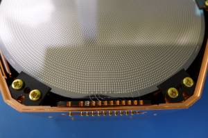 | 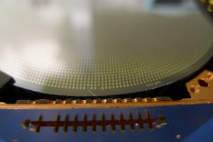 |
| Here I left Matt C's complicated hop-scotch bonds from pA to TES4. I added bonds from pB to TES3. One of these bonds was in contact with the pA bonds and caused a short, until I pushed the wire out of the way. The pD-TES2 bonds were removed and replaced with pC-TES2. | Here I simply replaced the bond from pin 6 (pC) to TES5. Previously this channel was reading open - now it reads unusually low at 27 Ω. |
| DIB1 Side 2 | DIB3 Side 2 |
|---|---|
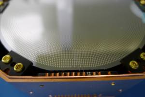 | 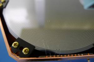 |
| Here the pB-tes10 and pC-tes9 bonds were removed, and pD-tes9 was bonded, and tes10 was shorted to tes9 | pA-tes11 was removed, and pB-tes11 was bonded instead. pA-tes8 was bonded using two stadiums with surgery to remove the connections on one side. tes8 is showing an ordinary resistance but tes11 is, like TES5, reading unusually low at 26 Ω. |
Interestingly the two outer ring channels, tes11 and TES5, are reading very low resistances. This was not seen in Matt Cherry's original wiring, which seems to be a coincidence, since both of these were reading open or nearly so, so they must have had poor connections. One of Matt C's originals was a complicated hop-scotch bond. Now both bonds are direct and not long and are not in danger of shorting with other bonds. So the low resistance of these channels seems to be real.
There are also two channels that are somewhat lower than the others, both a little above 100 Ω - and these turn out to be the B-ring channels, the second-to-outermost channels. So there is a clear pattern here - the outer ring channels have lower resistances. And the trend continues to the center, because the two center channels are almost the highest resistances.
| Position | Resistance [Ω] |
|---|---|
| A-ring (outermost) | 26, 27 |
| B-ring | 107, 131 |
| inner ring | 287, 301, 347, 392, 392 |
| center | 378, 420 |
| DIB4 Side 2 |
|---|
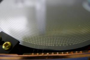 |
| I didn't do any modifications on this one, but the pin4 bond broke during handling. It will need to be fixed. Unfortunately this is a “hop-scotch” bond, it may be difficult for me to fix it. |
| 1710 | Return S101 to purge cabinet |
|---|