Previous Day
| | Status: clean tent is up, ready for deinstall. IVC is filled to near 1 bar with N2 but should be topped off a bit. All mixture in dump. MB vacuum jacket has been pumped out. |
| | G101c (SNOLAB HV prototype) arrived yesterday, one broken wirebond, no LEDs |
| 0905 | Tower (Cernox) = 299 K and flat |
Discussion between Matt, Allison, Nick re options for installing LEDs in source housing:
Idea: install source housing above detector and put LEDs in housing facing detector, somehow wire them to the LED lines from the detector DIBs
LED choice:
Use the loose DIB boards we have (there are 3 of them) that have LEDs installed on them, screw them into source housing
is there room to do this in the source housing?
these have not been tested, and some have broken bonds, would need to wirebond them
Use the IR LEDs that were used for the 150mm setup ← this option
would take several hours to mount the loose LEDs on boards
LED boards could be attached to source holder plate
source holder plate would need to be pointed away from detector, so we could not mount an internal Am source
In either case would probably want 3, at least 2 LEDs to illuminate detector (note only one side gets illuminated) ← plan on 4 to wire to the two DIBs whose LEDs map through the HV board
Wiring options:
LED ground wire simply attaches internally to source housing
need LED bias wire from source housing to connect to proper line leading to DCRC
wire to detector DIB, wrap around pin? probably not reliable
wire to unused tower face, plug into 30 mK stage
at the tower 4K stage extend a wire from unused tower face to stripline rerouting board to connect to LED bias line
wire to extender between side coax and 30 mK tower face plug. Maybe could solder directly to it. ← this option
Questions:
can DIBs with LEDs be attached to source housing? If so can the source holder also be installed?
either source holder plate would need to be removed or a section cut out of it
how easy would it be to attach LED boards (the ones used for the 150mm) to the source holder plate and solder ground connections?
seems easy, plenty of holes in plate, bolt and nut to hold board on
are we willing to leave out an internal source? we were thinking of doing so anyway
yes looks like we'll leave it out
can we figure out how to solder a wire to a pin on the side coax extender?
probably, can wrap around middle of pin and solder it on
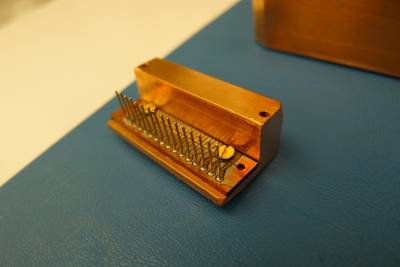 | 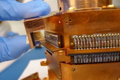 |
| Extender has long pins, could solder a wire directly to one of them |
From left to right (with tower upright), the tower face pins are numbered 1-16. Pin 9 and Pin 10 are LED1&2.
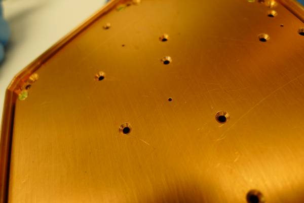 |
Lots of holes in source plate provide plenty of spots to attach LED boards
No space to attach a DIB unless source plate removed or a piece cut out of it |
| 1100 | Checking the accelerometer (CEM DT-178A) data from the shipping container of the detector received yesterday. Only 5 seconds worth of data from 9/19 is recorded. Checking the voltage produced by the internal battery, it's clear that the battery is dead, so presumably only 5 seconds of data was recorded before the death. Currently looking for a replacement battery so we can test out the accelerometer. |
| 1310 | Remove G101c from purge to inspect Side 2 bonding |
Detector mask and wirebonding (Paul Brink's original plan plus later notations): hv_umn_proposed_pads_160929.pdf
Two of the DIBs are thinner than standard, DIB2 and DIB4, because there are no flats on the detector at those positions. The semicircular depressions of the contact pads on the thin DIBs are deeper than for the standard DIB, and from something Matt C said I think it's probably a lot harder to wirebond onto them.
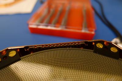 | 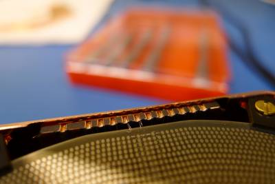 |
| Thin DIB with deep depressions | Standard thick DIB with shallower depressions |
The Side 2 connections for DIB4 are currently attached to pC and pD which are closer to the pads than pA and pB. So if we were to swap these connections around it would be difficult on this side.
| | DIB 4 Side 2: | DIB 1 Side 2: | DIB 3 Side 2: |
| Paul's diagram: | pA-TES7, pB-TES6 | pD-TES10 | pA-TES11 |
| Actual: | pC-TES8, pD-TES7, TES7-TES6ret, TES6ret-TES6 | pD-TES9, TES9-TES10ret, TES10ret-TES10 | pB-TES11 |
| 1739 | Place Cf source inside purge cabinet on top of HV Detector for overnight activation. |
Next Day