Table of Contents
Rebonding detector G101c (HV#2)
| HV#2 wiring from Run 61 | ||||
|---|---|---|---|---|
| pA | pB | pC | pD | |
| DIB1 | TES4 | TES3 | TES2 | TES9(-TES10) |
| DIB3 | n/c | TES11 | TES5 | n/c |
| DIB4 | n/c | TES8(-TES7-TES6) | TES1 | TES0 |
| Bold = Side 1, Italic = Side 2 “-” indicates a non-readout channel shorted to a readout channel for biasing purposes |
||||
In Run 61 we left three channels unconnected to readout. All the channels that were connected worked.
| HV#4 wiring from Run 62 | ||||
|---|---|---|---|---|
| DIB1 | TES4 | TES3 | TES2 | tes9(-tes10) |
| DIB3 | tes8(d4) | tes11 | TES5 | n/c |
| DIB4 | tes7 | tes6 | TES1 | TES0 |
| CAPITAL = Side 1, lowercase = Side 2 “-” indicates a non-readout channel shorted to a readout channel for biasing purposes |
||||
In Run 62 we managed to wire all but one channel on HV#4. Can we repeat this for HV#2?
| HV#2 in Run 61 |
|---|
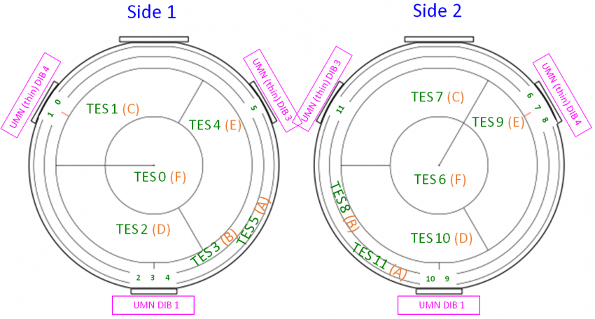 |
| G101c SNOLAB HV prototype channel layout. Also shown are the positions of the bond pads near each DIB. Two DIBs are thinner than standard because they are not at the detector flats. |
| HV#4 in Run 62 |
|---|
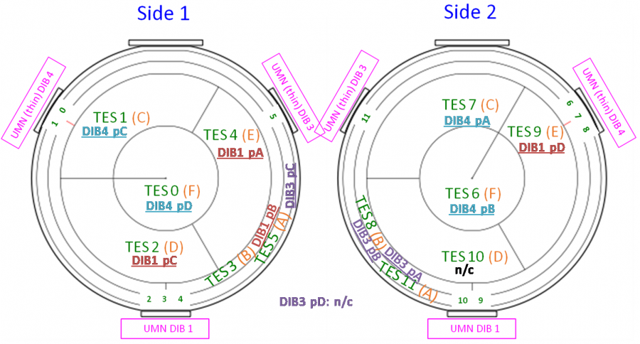 |
The trick for getting more channels with HV#4 was to attach wire bonds at DIB3 to a b-ring channel that doesn't have a bond pad at that DIB - the bonds extend to a couple of stadiums in the B-ring with surgery to disconnect those stadiums from one bias side.
Decision
For Run 66, we will probably not bother to connect more channels on HV#2. We are not planning to run in biased 2-sided mode, which would require floating the DCRCs. So we are only mostly going to read out Side 1, which is fully connected.
Reducing Shunt Resistance
We do intend to reduce the shunt resistances on the SQUETS for all the Side 1 channels in this run. We will reduce from 20 mΩ to 6.67 mΩ by connecting the “spare” 10 mΩ resistor in the SQUID chip in parallel with the existing 20 mΩ resistor.
We decided that with the 3 working channels on Side 2 we would experiment with different Rshunts. We can easily wirebond to either 20, 10, 6.67, or 0 mΩ. Here are some ways to do that:
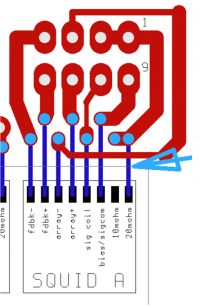 | 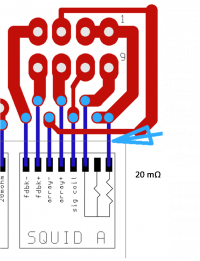 | 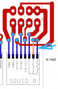 | 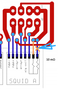 | 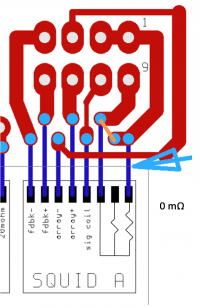 | 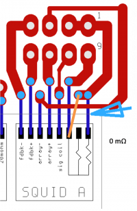 | 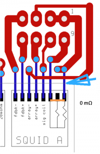 |
| The standard SQUID chip wiring diagram. Blue lines are standard wirebonds. | 20 mΩ wiring (no changes to standard bonding) | 6.67 mΩ wiring. New wirebond in orange. | 10 mΩ wiring. Original wirebond removed. | Three 0 mΩ wirings involving 1, 2 or 3 bonds. | ||
| Note that all bonds shown are actually bond pairs. | ||||||
We intend to wire the Side 2 shunts so that one channel is standard 20 mΩ, one is 10 mΩ, one is 0 mΩ using the 1-bond wiring option above (to test the smallest possible parasitic resistance), and one is 0 mΩ with the 2-bond or 3-bond option, to see if we can distinguish a difference between them.
| HV#2 (G101c) wiring | ||||
|---|---|---|---|---|
| pA | pB | pC | pD | |
| DIB1 | TES4 | TES3 | TES2 | TES9(-TES10) |
| DIB3 | n/c | TES11 | TES5 | n/c |
| DIB4 | n/c | TES8(-TES7-TES6) | TES1 | TES0 |
| Bold = Side 1, Italic = Side 2 “-” indicates a non-readout channel shorted to a readout channel for biasing purposes |
||||
| SQUET rewiring | |||||
|---|---|---|---|---|---|
| pA | pB | pC | pD | SQUET | |
| SQUET for DIB1 | 6.7 mΩ | 6.7 mΩ | 6.7 mΩ | 0 mΩ, 1-bond | ZC-68 |
| SQUET for DIB3 | n/c | 10 mΩ | 6.7 mΩ | n/c | ZC-74 |
| SQUET for DIB4 | n/c | 0 mΩ, 3-bond | 6.7 mΩ | 6.7 mΩ | ZC-31 |
| Bold = Side 1, Italic = Side 2 | |||||
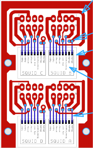 |
| This figure shows the channel layout on the SQUID card |