−Table of Contents
High Voltage Interface Board for iZip v6
by Nick Mast Edited by Derek Sincavage on 19/10/2021
Motivation
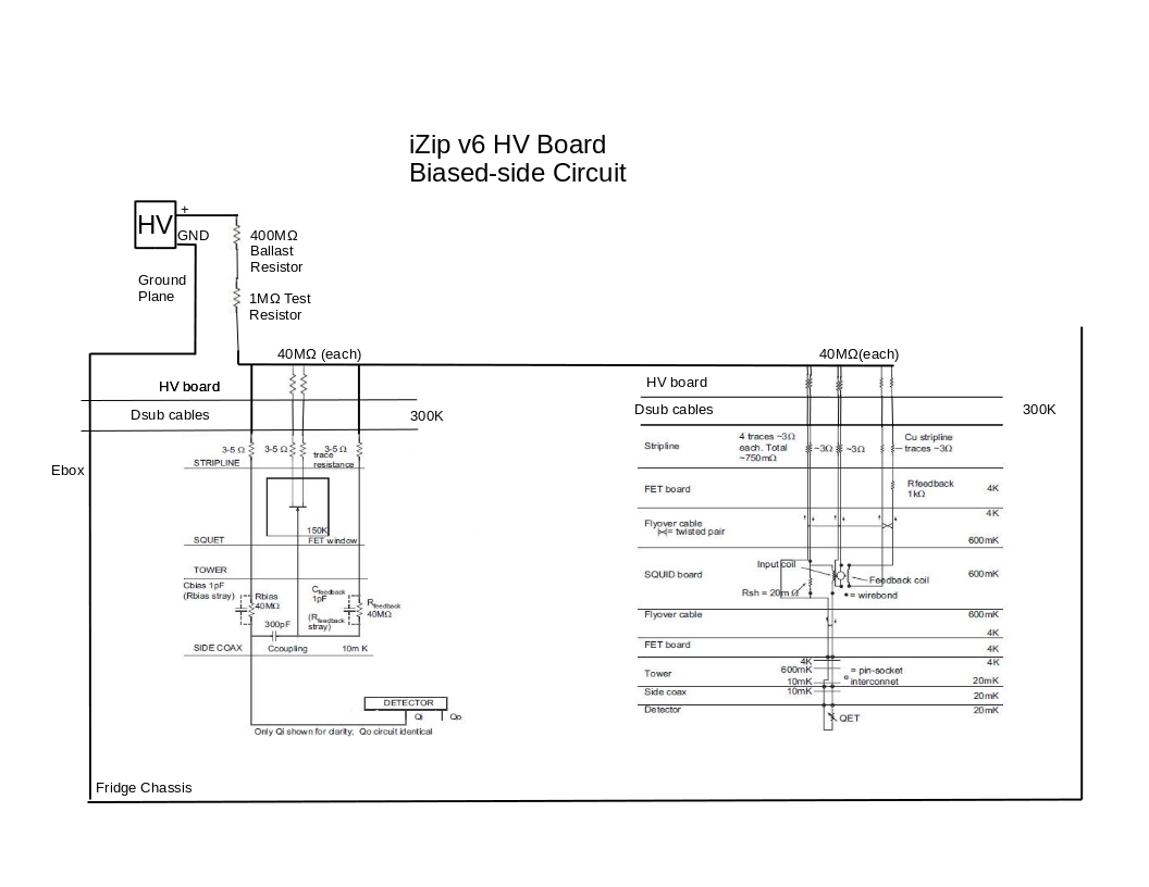
It was desired to bias iZip v6 detectors to voltages higher than what the DCRC was capable of(~ +/-13V). To do so, a circuit was designed to interrupt the relevant signal lines between the ebox and DCRCs and re-rout them to an external power supply while passing through normal signal lines to the DCRCs. The design was inspired by Jeter's CDMSlite board and Hassan's board for a charge only detector. Hassan had also done some early work on possible HV boards for iZip v6.
Design
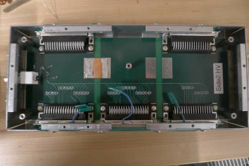
We presented a proposed design at several detector tower hardware meetings. The final design and board layout were completed and the boards were fabricated by Custom Circuit Boards. They were populated with components by hand in the lab. Note that a separate board was designed to bias each side of the detector.
| Figure 1: PCB Outline for High Voltage DCRC Interface Boards |
|---|
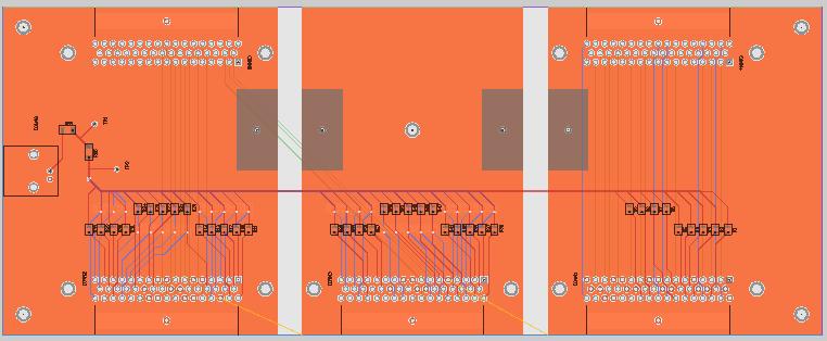 |
|Final Design Bias side 1 |Final Design Bias side 2 Board Pinouts
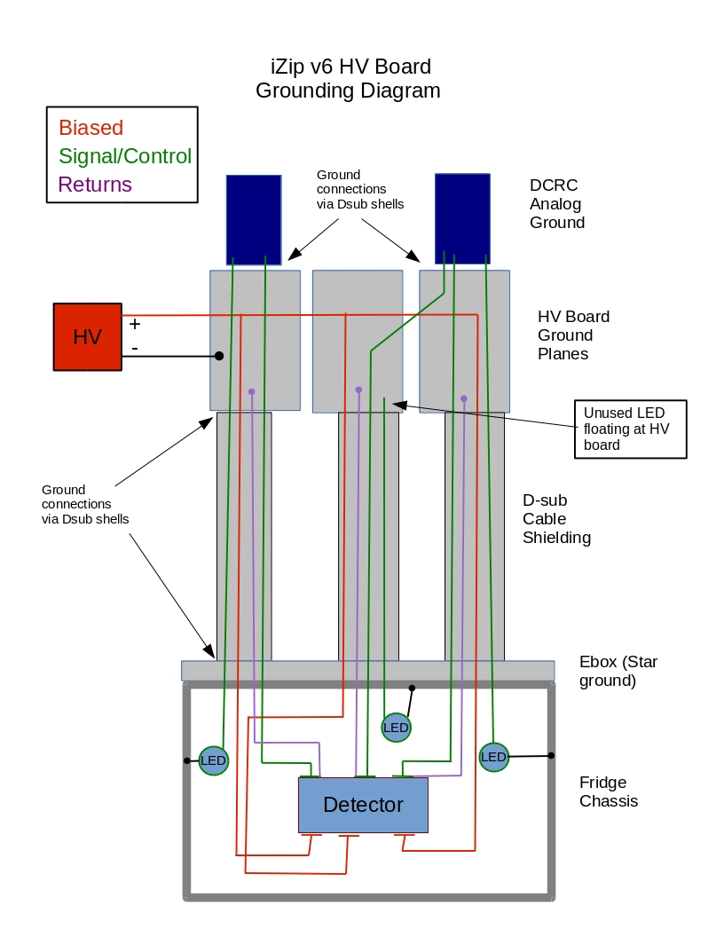
To help shield the traces from RF interference, the board has an internal ground plane and is housed in a metal box.
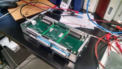
Because one entire side of the detector is biased, only 6 phonon channels need to be read out which means that only 2 DCRCs are required. The mapping of channels is as follows.
| Bias Side 1 | Bias Side 2 | |||||||||
|---|---|---|---|---|---|---|---|---|---|---|
| DCRC1 | DCRC2 | DCRC1 | DCRC2 | |||||||
| PA | PCS2 | PA | PBS2 | PA | PBS1 | PA | - | |||
| PB | PAS2 | PB | PFS2 | PB | PFS1 | PB | PES1 | |||
| PC | - | PC | - | PC | PCS1 | PC | PDS1 | |||
| PD | PDS2 | PD | PES2 | PD | - | PD | PAS1 | |||
| Qi | - | Qi | QiS2 | Qi | QiS1 | Qi | - | |||
| Qo | - | Qo | QoS2 | Qo | QoS1 | Qo | - | |||
| LED | LED DIB2 | LED | LED DIB3 | LED | LED DIB1 | LED | LED DIB2 | |||
Bias at the detector can be calculated as Vc = HV - [(Ri+Rt)/Ri]*[Rb/Rt]*Vt = HV - 440*Vt
Modifications
| It was discovered that the PCB design contained an error and the FET heater +/- and Tsense lines were not connected for the charge readout channels. This is was mended by soldering small wires connecting the appropriate DSub pins on the underside of the board. Charge readout seemed to work properly thereafter. |
| It was discovered later that the channel map used in constructing this device was incorrect for the detectors used. See Run 57 Summary for more info. The result is that one channel was biased which shouldn't have been, and one wasn't biased which should have been. A second board was constructed out of a warm-end stripline diverter to reroute these two channels, effectively undoing the mapping error built into the HV board. Note: for later HV-prototype detectors the wirebonding was done to match the existing boards, so that this correction is not necessary. |
| 13/6/2016 | While testing USD1, it was found that, with only DIB1 and DCRC1 connected, the hv board-box combo picks up a ~60Hz noise signal, even when disconnected from the HV source. This was found to be alleviated by connecting the box, which was initially floating, to the HV board ground plane. |
|---|---|
| 22/2/2017 | The side 2 HV board was modified to remove biasing from the Connector 2 charge lines. This was done because shorts to chassis in the cold end of these lines were thought to be causing high leakage currents. This was accomplished by removing the QI/QO related HV bias resistors. The resistor numbers are R30, R31, R32, R35, R37, R40, R43, R47. |
| 30/3/2017 | The side 1 HV board was also modified to remove biasing from the Connector 1 charge lines. This was accomplished by removing the QI/QO related HV bias resistors. The resistor numbers are R11, R13, R18, R48, R51, R52, R55, R56 |
| 19/4/2017 | Modified side 2 HV board to bridge the ground planes spanned by the crossover channel. Previous bench tests indicated that this may improve the crossover channel noise. |
| 15/11/2017 | Modified side 2 HV board to remove biasing from unused channels for run66. Details of the configuration can be found here. |
| 3/5/2018 | Replaces some resistors to match HV4 wiring for run68. Configuration is here: hv_board_wiring_run068.xls |
| 27/3/2019 | Remove all resistors except those on DIB4PA to bias only this channel which is connected to the contact free electrode in run69. Configuration here: hv_board_wiring_run069.xls |
| 23/4/2019 | Remove all resistors from Side 2 HV board except DIB4 QET A (R51) and a single DIB4 QET A ret (R25). Configuration here: hv_board_wiring_run070.xls |
| 19/10/2021 | Re-install all resistors from Side 2 HV board except charge channels. Configuration here: hv_board_wiring_run075.xls |
| 8/2/2022 | Attach jumper wires on Side1 HV board connecting CONN1 LED pins to CONN4 (HV1) LED pins. The CONN1 LEDs were left open on the board design but for Run 75 we want them connected. |