Passive Johnson Noise
Theory
This run featured SQUID cards with modified shunt resistors to reduce the passive Johnson noise in the TES circuits. The passive Johnson noise depends on the resistance and temperature of the shunt and parasitic resistances. As described in detail here, the low frequency level of the superconducting noise can be used to measure this Johnson noise. The superconducting noise level is:

The numerator is the Johnson Voltage noise on the resistors. Note that lowering the Johnson Voltage noise by reducing shunt or parasitic resistances will actually increase the SC noise level due to the SC circuit impedance. In transition, however, the circuit impedance is dominated by the TES operating resistance and feedback factors.
 To understand the noise signal, we need a model for where the parasitic resistances are located. The most often cited parasitic resistance culprits in our setup are the Al wirebonds and the milmax pin connections. The diagram on the right shows these bonds and the temperature stages at which they are located. In summary, we have:
| On Rsh branch | On TES branch | ||
|---|---|---|---|
| Resistor | Temp stage | Resistor | Temp stage |
| Rsh | Tsquid | 1xRbond | Tsquid |
| 1xRbond | Tsquid | 2xRpin | Tsquet |
| 4xRpin | Tdet | ||
| 2XRbond | Tdet | ||
Note that the detector and squid temperatures should be below the Al superconducting temperature of 1.2K, so the wire bonds should have 0 resistance and not contribute to the Johnson noise. Besides the shunt resistor, the dominant parasitic passive Johnson noise contributor should be the Milmax pins connecting the squet card to the tower bottom, which is nominally at 4.2 K.
Combining all of these gives expressions for the total parasitic resistance on each branch:
Rp_shunt = Rbond
Rp_TES = 6xRpin + 1xRbond(@Tsquid) + 2xRbond(@Tdet)
Measurement
Using these parameters and the assumed exact values of the shunt resistors, one can model the passive Johnson noise using the above equation with the free parameters being the bond and milmax resistances and the squet and squid temperatures. This noise was measured for 3 different Rsh values:
| Rsh (mΩ) | Series | Tower (mK) | Channel | I_PJN,0,SC (pA/rtHz) |
|---|---|---|---|---|
| 20 | 07161102_1556 | 32 | S1PA,PB,PC,PE,PF | 45.0 ± 0.9 |
| 6.67 | 07171219_1202 | 55 | S1PA-PF | 65.1 ± 2.9 |
| 6.67 | 07171216_2307 | 22 | S1PE | 68.7 ± 1.3 |
| 0 | 07180103_1403 | 22 | S2PB | 78.3 ± 1.3 |
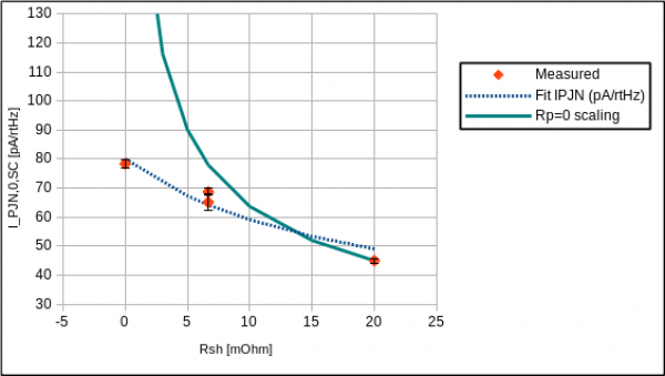
These data were fit to the above noise model with 4 free parameters: Rbond, Rpin, Tsquid, and Tsquet. The detector temperature was fixed, but makes no difference in the fit parameters. A simple chi-squared minimization was done in Excel, the results of which are shown below. Also shown for reference is the noise scaling (relative to the 20mΩ level) which would be expected without any parasitic resistance.
 |
| Fit Parameters | |
|---|---|
| R_bond | 0.05 mΩ |
| R_milmax | 1.88 mΩ |
| T_squid | 1.39 K |
| T_squet | 3.97 K |
As can be seen, the fit values are reasonable, though there is certainly some degeneracy in the fit which is hard to account for. However, trusting this fit indicates that the squid card actually runs hotter than the Al transition temperature, so the wire bonds there are not superconducting and do contribute slightly to the parasitic resistance. These results indicate that the parasitic resistances are:
Rp_shunt = Rbond = 0.05 mΩ
Rp_TES = 6xRpin + 1xRbond = 11.33 mΩ
Comparison to IbIs
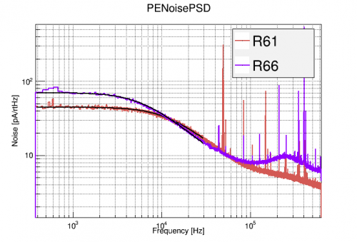
The IbIs analysis of R61 and R66 have been done here. Re-interpretting the ratios as being dependent on exact shunt resistances and unknown (but constant) parasitic resistances on the shunt and TES branches, Rp_sh and Rp_TES, we have.
| Run 61 | Run 66 | ||||
|---|---|---|---|---|---|
| DCRC chan | Det chan | Rp_TES/(Rsh61+Rp_sh) | (Rn+Rp_TES)/(Rsh61+Rp_sh) | Rp_TES/(Rsh66+Rp_sh) | (Rn+Rp_TES)/(Rsh66+Rp_sh) |
| DCRC1pA | Side1 pE | 0.38 | 3.779 | 1.154 | 10.732 |
| DCRC1pB | Side1 pB | 0.729 | 5.167 | ||
| DCRC1pC | Side1 pD | 0.531 | 3.125 | 1.42 | 9.923 |
| DCRC3pB | Side1 pA | 0.47 | 4.308 | 2.005 | 16.453 |
| DCRC3pC | Side1 pC | 0.372 | 4.413 | 1.432 | 11.887 |
| DCRC3pD | Side1 pF | 0.569 | 3.4 | 1.869 | 10.4 |
Now, for each run, we can take subtract the first ratio from the second, to get the Rn/(Rsh+Rp_sh) ratio. Then, assuming the normal resistances are constant across runs, we can find the ratio of Rsh+Rp_sh of the two runs and, assuming the exact values of R_sh, find Rp_sh. These values are consistent with 0. Finally, these can be used to calculate the remaining parasitic resistance on the TES branch for each run.
| DCRC chan | Det chan | Rn/(Rsh61+Rp_sh) | Rn/(Rsh66+Rp_sh) | (Rsh61+Rpsh)/(Rsh66+Rpsh) | Rp_sh (mΩ) | Rp_TES_R61 (mΩ) | Rp_TES_R66 (mΩ) |
|---|---|---|---|---|---|---|---|
| DCRC1pA | Side1 pE | 3.399 | 9.578 | 2.818 | 0.663 | 7.852 | 8.462 |
| DCRC1pB | Side1 pB | 4.438 | |||||
| DCRC1pC | Side1 pD | 2.594 | 8.503 | 3.278 | -0.818 | 10.186 | 8.309 |
| DCRC3pB | Side1 pA | 3.838 | 14.448 | 3.764 | -1.848 | 8.531 | 9.668 |
| DCRC3pC | Side1 pC | 4.041 | 10.455 | 2.587 | 1.728 | 8.083 | 12.026 |
| DCRC3pD | Side1 pF | 2.831 | 8.531 | 3.013 | -0.049 | 11.352 | 12.374 |
Averaging over both runs then gives values of
Rp_sh = -0.06 ± 1.37 mΩ
Rp_TES = 9.68 ± 1.71 mΩ
These are consistent with the values obtained from fitting the PJN noise above which lends credence to both methods.