Run 64 Summary
Detector
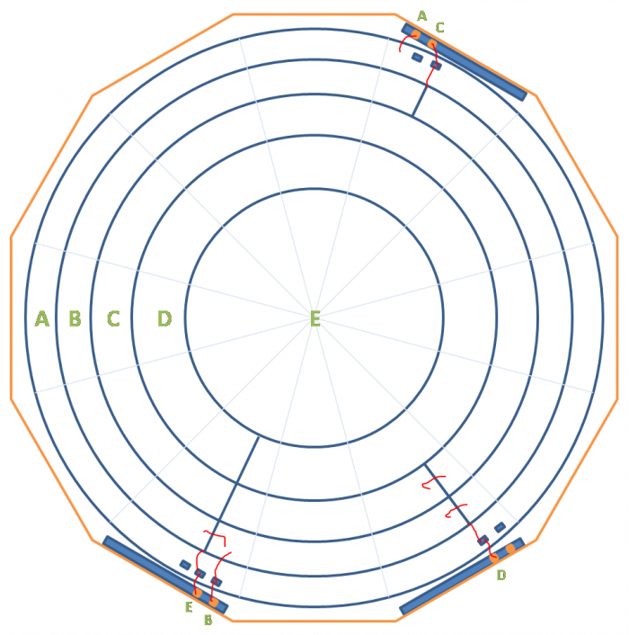 |
| Wirebonding plan for S1502 |
Wiring Plan for detector and switchboards
| DIB1qI | qA - outer |
|---|---|
| DIB4qI | qB |
| DIB1qO | qC |
| DIB3qO | qD |
| DIB4qO | qE -inner |
Contact free bias is run through DIB1 QETA + QETA ret lines. A pair of bias resistors in series on the DIB 1 switchboard allows for the leakage current to be measured, similar to the way it is done with the HV board.
- The large bias resistor is 10.95 MΩ
- Leakage measurement resistor is 1.03 kΩ
- This gives the formula for the bias at detector as: V_det = V_set - 1.06E4*V_leak
The voltage across the crystal is not the same as that applied to the detector as a whole because there is a voltage drop across the vacuum gap. By treating the gap and crystal as parallel plate capacitors in series, one obtains.
- V_crystal = V_det/(1+ε_Si/ε_0 * d_gap/d_Si)
- ε_Si/ε_0=11.68 (Wikipedia), d_gap=0.037“±0.004” (2017/09/08), and d_Si=1“
- V_crystal = V_det*(0.70±0.03)