 |
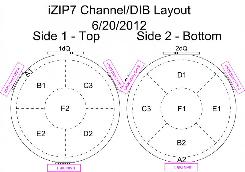
Original wiring proposal by Matt F:
- zp2_geizip_pathfinder_wiring.pdf
- zp2_geizip_pathfinder_wiring.pptx
| pA | pB | pC | pD | |
|---|---|---|---|---|
| DIB1 | Side1 pD | Side1 pF | Side1 pE | Side2 pB |
| DIB3 | Side2 pA | Side2 pC | Side1 pA | Side1 pC |
| DIB4 | Side1 pB | Side2 pE | Side2 pF | Side2 pD |
| proposed | ||||
| G132 aka ZP#2 aka Ge iZIP Pathfinder |
|---|
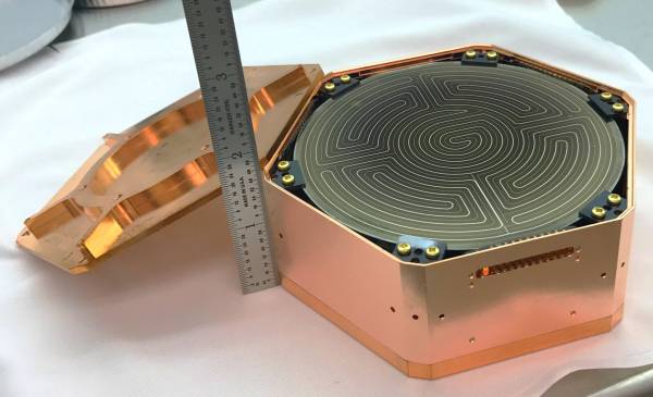 |
Link to notes on the packaging of G132 (on SLAC Confluence)
Matt Cherry's packaging notes above indicate that on one DIB (UMN DIB4) he rearranged the channels because some DIB traces were not continuous with the pins. In his notes he uses the TES0, TES1… labeling for channels and an unknown labeling of the DIBs which I translate below:
Matt C didn't indicate which physical charge channels (inner versus outer) map to which DIB pins. I had suggested that maybe he should swap them so that the bonds didn't cross one another, but his notes don't show whether he swapped them or not. However after opening the housing I could see that he has not swapped the innner/outer connections. The bonds are also not crossing - so he must have found a different way to bond them than I suggested.
| pA | pB | pC | pD | qI | qO | LEDs | |
|---|---|---|---|---|---|---|---|
| DIB1 | Side1 pD | Side1 pF | Side1 pE | Side2 pB | Side2 qI | Side2 qO | Pin9/10 = Side1/2 |
| DIB3 | Side2 pA | Side2 pC | Side1 pA | Side1 pC | Side1 qI | Side1 qO | n/c |
| DIB4 | | | | | n/c | n/c | n/c |
| Matt C's Wiring | |||||||
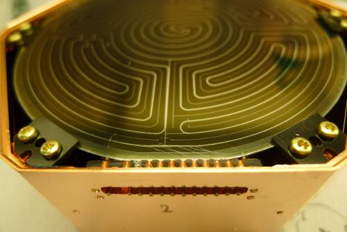
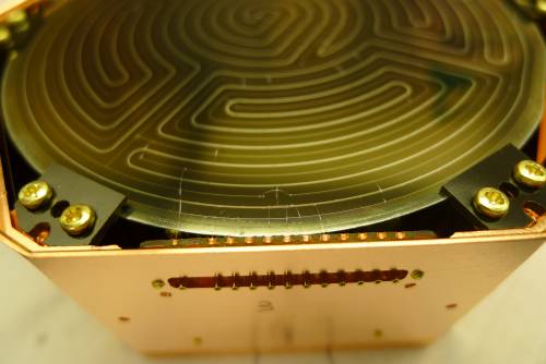
Matt C indicated that the oversized detector touches all three DIBs. He has Kapton between the detector and DIBs to prevent shorting. According to his room temperature measurements the channels measure ~ 100 Ohm to chassis, much less than usual. It is hoped that this shorting will disappear at low temperatures. Here are Matt C's channel measurements:
UMN DIB1
  Channel A: - 73.0 Ohm
  Channel B: - 82.8 Ohm
  Channel C: - 58.7 Ohm
  Channel D: - 11.3 Ohm
  LEDs: present
  Charge: - QiQo 55.0ohm - QoQi 56.1 Ohm
UMN DIB3
  Channel A: - 8.5 Ohm
  Channel B: - 23.9 Ohm
  Channel C: - 10.8 Ohm
  Channel D: - 29.4 Ohm
  LEDs: Not Present
  Charge: - QiQo 42.8ohm - QoQi 35.1 Ohm
UMN DIB4
  Channel A: - 38.4 Ohm
  Channel B: - 81.5 Ohm
  Channel C: - 76.3 Ohm
  Channel D: - 27.8 Ohm
  LEDs: Not Present
  Charge: Not Used
| Side 1 DIB1 | Side 1 DIB3 | Side 1 DIB4 |
|---|---|---|
 |  | 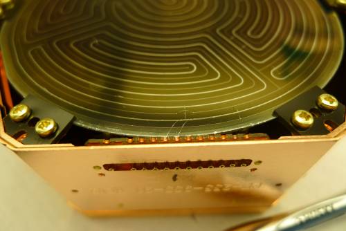 |
| Side 2 DIB1 | Side 2 DIB3 | Side 2 DIB4 |
|---|---|---|
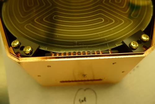 | 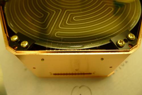 | 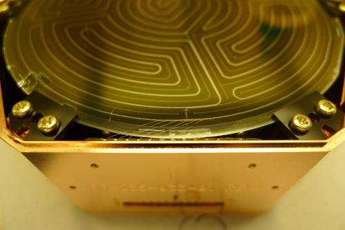 |
Error in wiring diagram:
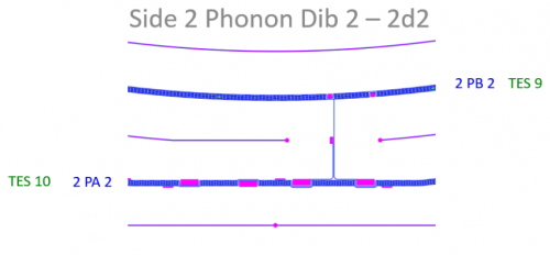
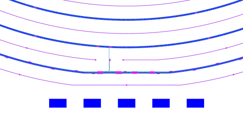
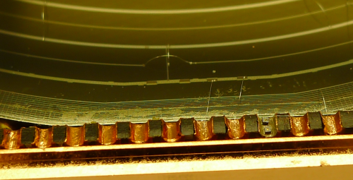
The slide show I used to create the wiring plan, zp2_geizip_pathfinder_wiring.pdf, was based on a slide show from Paul Brink that I modified. It has images from the mask diagram, zooms of regions near each DIB on each side. But if you compare the slide show to the iZIPv7 mask diagrams found at https://confluence.slac.stanford.edu/display/CDMS/Fourinch_iZIP_MIT, you'll find that one slide, Page 9, does not agree with the mask diagram. It seems to be a mirror image. This is Side 2 DIB1. The photo above shows that the actual detector agrees with the mask on Confluence, not the image in the slide show. This resulted in an error in the wiring. DIB1 pD was supposed to be connected to Side2 pB, but instead it's connected to Side2 pA. That means nothing is connected to Side 2 pB, and two DIB channels are connected to Side2 pA (both the intended DIB3 pA and the accidental DIB1 pD).
This explains one mystery - why were there two channels that showed a strong short to chassis after we cooled down? It's actually only one: Side2 pA, but it's connected to two DIB channels.
| pA | pB | pC | pD | qI | qO | LEDs | |
|---|---|---|---|---|---|---|---|
| DIB1 | Side1 pD | Side1 pF | Side1 pE | Side2 pA | Side2 qI | Side2 qO | Pin9/10 = Side1/2 |
| DIB3 | Side2 pA | Side2 pC | Side1 pA | Side1 pC | Side1 qI | Side1 qO | n/c |
| DIB4 | Side2 pE | Side2 pF | Side2 pD | Side1 pB | n/c | n/c | n/c |
| Matt C's Wiring. Note that due to an error, Side2 pB is not connected. Two DIB channels are connected to Side2 pA. | |||||||
| Side 2 DIB1 | ||
|---|---|---|
| From Paul's slideshow | From mask diagram | Actual photo |
 |  |  |