2020/01/22 (Tuesday)
G101c is currently at TAMU with Mark Platt to have its Side 2 channels etched away.
Last Friday Mark called to warn me. He saw that some of the Side1 bond pads had many wirebond stubs on them - clearly left over from my repairs/modifications. The problem with that is that the photoresist that covers Side 1 in order to protect it from the etching will not entirely cover these stubs, and the etch will eat away a little circle of the pad for each stub. Mark fears that this will make one or more pad unusable. He gives it a 50% failure rate.
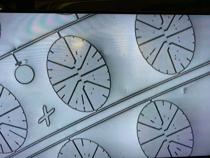
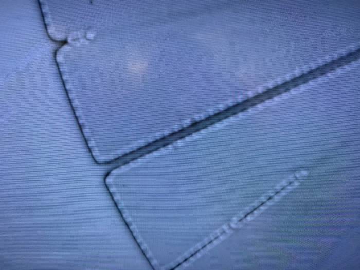
Today Mark emailed results of the Side 2 etch, and was concerned that there were remaining structures. Apparently they etched deep trenches (500-600 nm) when fabricating G101c at TAMU. But Rupak said it was probably not a problem - it just means that there will be unevenness on that side. The metal was successfully removed. Below are a couple of pictures from Mark of the remaining structures on Side 2 after etching.