2015/08/13 (Thursday)
| Overnight status: fridge at base. MC remained close to 26 mK. Circulation pressure rose to about 200 mbar by 4:30 then stabilized. | |
| 0915 | MC/Tower = 25.8/33.7 mK. Cold plate = 136 mK. Still = 1.05 K / 0.095 mbar. G1/G2 = 110 mbar. 1K Pot = 1.75 K / 28 mbar. |
| 1045 | Set up DCRCs as in the last run: DIB1/2/3 → 10MHz filter/none/none → DCRC55/33/50. Zap SQUIDs and apply previous SQUID/QET settings. |
| 1130 | DIB3pC pulses looked a little strange, like rain was dripping off of them. We tried to set it up with a test signal to look at the SQUID modulation curve but in various ways DCRC50 seemed to not be responding. Restarted DCRC50 and re-zapped. After two restarts, pC looked OK. |
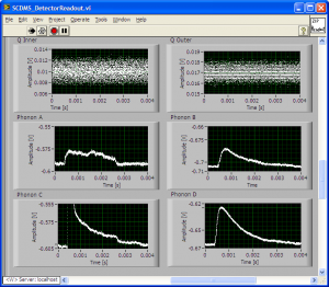
| 1300 | funny DCRC behavior. DIB2 pB showing upside down pulses. They can be made upright by setting the amplifier to inverting, or switching the QET bias from negative to positive. Either way this is non-standard, so DCRC must be confused. Restarting DCRC got it back to normal. |
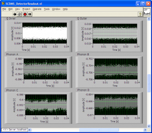
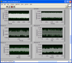
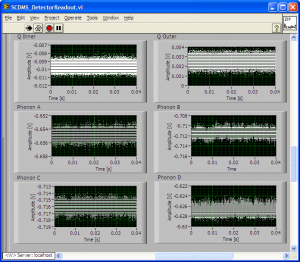
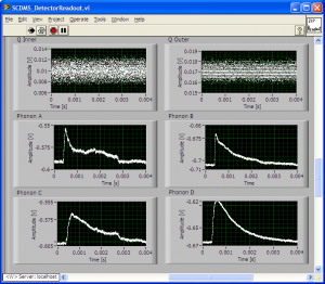
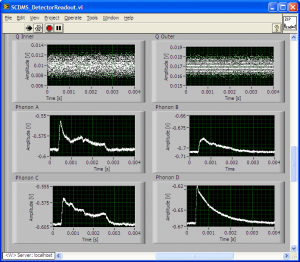
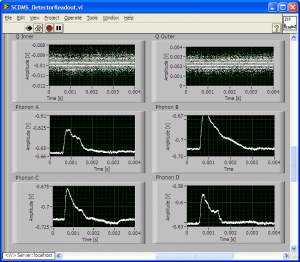
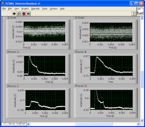
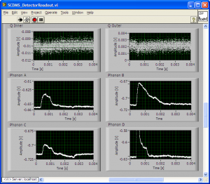
| 1435 | Took some snapshots of pulses and low-frequency noise: |
| Noise | |
|---|---|
| DIB1→filter→DCRC55 | |
 | |
| DIB2→DCRC33 | |
 | |
| DIB3→DCRC50 | |
 |  |
| Pulses | ||
|---|---|---|
| DIB1→filter→DCRC55 | ||
 |  |  |
| DIB2→DCRC33 | ||
 |  |  |
| DIB3→DCRC50 | ||
 |  |  |
| 1500 | Setting up HV board. |
|---|
| HV board on top of breakout box, DCRC side | HV board on top of breakout box, DIB cable side | DIB cables at ebox |
|---|---|---|
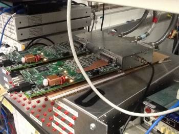 | 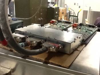 | 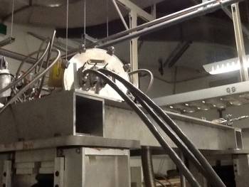 |
| 1515 | The HV board is designed so that the casing is isolated from the D-sub shells. However, the weight from the cables or DCRCs can cause the shells to come in contact with the casing. We carefully inserted the DCRCs and supported them with a pad of paper to prevent contact with the shell. The cables were attached to the top of the bench shelf with cable ties and adjusted for stress relief so that the shells weren't in contact with the casing. |
|---|---|
| 1530 | Setup: HV shorted, so that Side 2 is grounded. DCRC50/55 → HV slot 1/2. |
| HV board connected channels | ||
|---|---|---|
| HV channel | DIB channel | Detector channel |
| HV1 pA | DIB1 pA | S1 pB |
| HV1 pB | DIB1 pB | S1 pF |
| HV1 pC | DIB1 pC | S1 pC |
| HV1 pD | ||
| HV1 Qi | DIB1 Qi | S1 Qi |
| HV1 Qo | DIB1 Qo | S1 Qo |
| HV1 LED | DIB1 LED | LED DIB1 |
| HV2 pA | ||
| HV2 pB | DIB3 pC | S1 pE |
| HV2 pC | DIB2 pC | S1 pD |
| HV2 pD | DIB2 pD | S1 pA |
| HV2 Qi | ||
| HV2 Qo | ||
| HV2 LED | DIB2 LED | B2 pE |
| 1530 | Initial observations: we were able to see SQUID modulation curves on HV1 pA, pB, and pC, not on pD, which makes sense. In the HV1 charge channels we see only a flatline: these should show noise at least. Heating the FETs (wr 30 0900) didn't help. Turning off the FETs (wr 30 0) shows the sort of FETs-off noise we are used to - but this is also seen in HV2, whose charge channels are not connected to anything. So something seems wrong with the charge connections on the HV board. |
|---|
| 1620 | Commence LHe transfer (26.4%). |
|---|---|
| 1700 | Cease LHe transfer (95.8%). |
| 1749 | Fill LN2 cold trap full. |