2019/11/12 (Tuesday)
| Setup | DIB1/2/4 → 3.2 MHz filters → cable 1/2/3 → gender changer 1/2/3 → movable source controller/board with external Feedback resistor/nothing → DCRC55(1)/DCRC33(2)/DCRC50(3) |
|---|---|
| 0920 | Tower/MC/Coldplate = 36.4/30.6/192 mK, Still = 1.52 K/ 0.130 mbar / 0 mW, G1/G2= 191/161 mbar, 1K Pot = 1.66 K / 32±2 mbar. MB= 65.7% |
| 0925 | Fill LN2 cold trap bath. |
| 1040 | DCRC2pD has some ugly noise, maybe we need to zap SQUIDs |
| 1040 | Zap all SQUIDs using tool on DCRC Control UI (seems to work this time) |
| 1055 | After zap, Tower cooled back to 40 mK, but then got hotter again for some reason, → 43 mK and rising. I guess the DCRCs are in a bad state. Lame. |
| 1055 | Doesn't look like the bad state we were getting into the other day at -/+ biases, because DCRC1 charge channels look fine. But let's try raising DCRC1 qI/O biases from 0V to 2V anyway, see if that “fixes” things. |
| 1100 | Temperature coming down, huh. Not very quickly though. Set DCRC1 charge bias back to 0V. |
| 1110 | Tower has fallen to 37.3 mK, seems maybe to be approaching previous base |
| 1115 | Tower = 36.6 mK, so I gues50s it's healthy. Let's adjust phonon offsets. Last night's data was mostly railed, we'll take some more. |
| 1125 | Phonon channels look ok but DCRC2pD has some ugly noise, let's take it out of the triggering. |
| 1128 | Start 2x S1/S2=+4/-4 V loop of 30 min Bkg data series with unchanged phonon settings, Driver gain = 1, with 1000 initial randoms, with 30s flashes and 30 min cooldowns trigger on DCRC2pA/B/C = 8/8/8 ADC using sequence take_and_flash_loop.msl (with negative DCRC2 LED bias) |
| 1159 | While still running this series, check DCRC1 biases using exposed leads on diverter boards. QI/QO = Switch number 9-3 / 7-4. On DIB1, these both read -9.5 V when they should be +4V! This can probably explain a lot of the weird behavior we've seen thus far. |
| 1202 | Stop sequence just after flash. DCRC 1/2 (QI/QO) = (-10.5/-10.5)/(-0.24/-0.26) V |
| 1230 | Telnet to DCRCs. Display calibration register values on RevC.1 using the command cald 1. For RevC, the calibrations are done in dcrc_driver. |
On DCRC1, the charge cals are
A=00  D=8067  QinnerOffset  Qinner bias is zero with this setting, DAC
A=01  D=01AB  QinnerSlope   The Qinner bias setting slope, uV/DAC
A=02  D=8018  QouterOffset  Qoute50r bias is zero with this setting, DAC
A=03  D=01AB  QouterSlope   The Qouter bias setting slope, uV/DAC
and on DCRC3 they are
A=00  D=80A3  QinnerOffset  Qinner bias is zero with this setting, DAC
A=01  D=01A8  QinnerSlope   The Qinner bias setting slope, uV/DAC
A=02  D=8027  QouterOffset  Qouter bias is zero with this setting, DAC
A=03  D=01AC  QouterSlope   The Qouter bias setting slope, uV/DAC
The ODB has all biases set to 0, but the relevant registers on DCRC1 QI/QO = 2000/2000 while DCRC3 QI/QO = 80A3/8027.
| 1237 | Set DCRC1 QI/QO to 0V via telnet by writing the calibration offset values for QI/QO = 8067/8018 to registers 0x59/0x5A. Measuring QI, QO bias at the diverter board indeed shows it is now set to 0.00/0.00 V! Set DCRC1 QI/QO bias = 0/0 in ODB, registers are unchanged50. Set DCRC1 QI/QO bias = 0/0 using DCRC_UI, registers are unchanged. Set DCRC1 QI/QO bias = 1/1 in ODB, read registers 0x59/0x5A = 2249/2249 and measure QI/QO = -10.3/-10.3 V. Set DCRC1 QI/QO bias = 0/0 in ODB, read registers 0x59/0x5A = 2000/2000 and measure QI/QO = -10.5/-10.5 V. |
|---|---|
| 1248 | Set registers 0x59/0x5A = FFFF/FFFF and measure QI/QO = 13.9/14.0 V. Set registers 0x59/0x5A = 8067/8018 and measure QI/QO = 0.00/0.00 V. So DCRC1 is doing the correct thing, but the ODB is sending the wrong thing to the charge bias registers. |
| 1253 | Set DCRC1 AmpOffset (V) = 0/0 and repeat test done at 1237 with the same results. |
| 1256 | Restart triggerfe2, towerfe3_01, and dcrc_driver01. Set DCRC1 QI/QO bias = 1/1 in ODB, read registers 0x59/0x5A = 898D/893E and measure QI/QO = 1.00/1.00 V. Set DCRC1 QI/QO bias = 0/0 in ODB, read registers 0x59/0x5A = 8067/8018 and measure QI/QO = 0.00/0.00 V. Restarting the programs fixed it somehow. |
| 1302 | Okay, things may be working again. Flash detector for 30s. |
| 1333 | Seeing phonon pulses and little to no charge pulses. DCRC1 registers read 0x59/0x5A = 8067/8018. Several phonon channels are railed, adjust them now. |
| 1343 | Start 1x S1/S2=+4/-4 V loop of 30 min Bkg data series with unchanged phonon settings, Driver gain = 1, with 1000 initial randoms, with 30s flashes and 30 min cooldowns trigger on DCRC2pA/B/C/D = 8/8/8 ADC using sequence take_and_flash_loop.msl |
| 1345 | Read DCRC1 registers 0x59/0x5A = A4FF/A4B0 |
| 1500 | Start 1x S1/S2=-4/+4 V loop of 30 min Bkg data series with unchanged phonon settings, Driver gain = 1, with 1000 initial randoms, with 30s flashes and 30 min cooldowns trigger on DCRC2pA/B/C/D = 8/8/8 ADC using sequence take_and_flash_loop.msl Read DCRC1 registers 0x59/0x5A = 5BCF/5B80 |
| 1545 | Power arduino and connect to it via telnet. Then turn on the motor controller power supply to 8V. Set the dwell to 8 ms. Set the current step position with wr currstep 278. |
| 1549 | Move to step 356, the middle of the first blocker, with command mvto 356. Tower spikes to 1.51 K. \\Also have the oscilloscope connected across one of the motor coils to monitor voltage. The signal is a series of sharp spikes instead of the expected square wave drive signal. |
| 1553 | Tower = 220 mK Power down motor power supply, then disconnect from and power down arduino. |
| 1608 | Tried moving the warm motor, saw expected 5 V square wave on the oscilloscope. Reconnecting both scope channels to the fridge motor leads at the arduino for future testing in case connection was bad in the first move. We think it might have not been properly connected on the first test leading to the bad signal. |
| 1610 | Tower = 60 mk |
| 1635 | Fill LN2 cold trap full. |
| 1640 | Check and reset all phonon channels to good states. |
| 1652 | Start 4x S1/S2=+4/-4,-4/+4 V loop of 30 min Bkg data series with unchanged phonon settings, Driver gain = 1, with 1000 initial randoms, with 30s flashes and 30 min cooldowns trigger on DCRC2pA/B/C = 8/8/8 ADC using sequence qbias_pm4_mp4_loop.msl |
| 1656 | Tower = 40 mK |
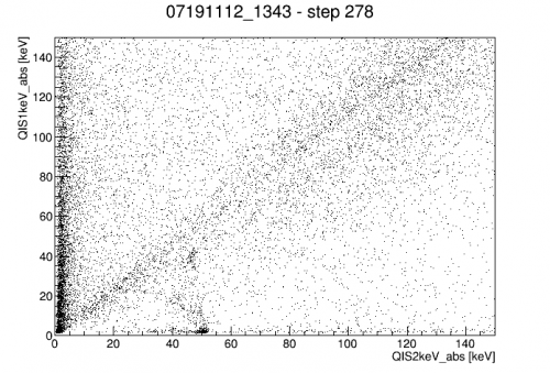
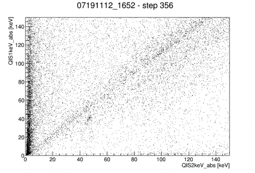
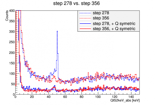
Quick look at 07191112_1652 QI plot with rough absolute calibration indicates some 60keV is still present. However there is significantly less 60keV near side 2 after the move. The lower plot compares the QIS2 spectrum in the two positions with and without a charge symmetry cut.
 |  |
 |
|
In any event, the total phonon signal fell after turning on the motor. Note the post-move PTINTall quantity has scaled up by ~2.5.
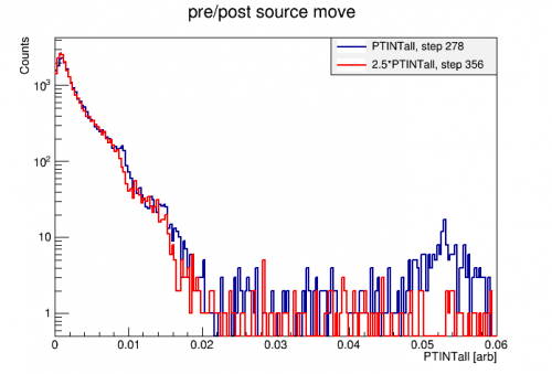 |
Took a look at the reduction in phonon collection efficiency channel-by-channel. Selected charge-symmetric 60keV events. Here's the breakdown:
| Side 1 | relative PCE | Side 2 | relative PCE | |
|---|---|---|---|---|
| pF | 0.58 | pF | 0.54 | |
| pE | 0.46 | pE | 0.44 | |
| pD | 0.44 | pD | 0.50 | |
| pC | 0.40 | pC | 0.43 | |
| pB | 0.47 | pB | 0.35 | |
| pA | 0.41 | pA | 0.34 |
The relative PCE for after versus before the move seems to be systematically higher for the center channels, otherwise it's pretty much the same for the other channels. Consistent with the overall 0.40 that the scaled spectrum shows.
Looking at these plots there's another strange observation - most channels show a single peak when you select the charge-symmetric 60keV events, but the two center channels (pF on Side1 and Side2) show double peaks.
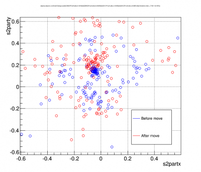
Side2pD is a high outlier; Side2pB is a low outlier. This is consistent with the idea that the source moved in the +y direction, toward the motor. There have been a few hints that this is the direction we have been moving it.