2019/02/18 (Monday)
| 1410 | Remove G101c from source safe, where it has been sitting with the Cf source for neutron activation |
|---|---|
| 1415 | Bring G101c into clean room. |
| 1440 | Begin removing wirebonds from Side 2. This is the side opposite the DIB slots (away-from-tower side). Used tweezers and magnifying glass. When I dropped a bond on the detector I removed it with a methanol-damped piece of wipe. |
| 1455 | Finish removing wirebonds. Double-bag detector. |
| 1505 | Return G101c to source safe to continue activation with Cf source. Detector is in poly/lead-lined lower compartment with Cf source, which is in its poly holder. |
| Wirebond count | ||
|---|---|---|
| Near DIB 1 | Near DIB 4 | Near DIB 3 |
| from DIB Chan D to pads on right. | from DIB Chan B to pads on left | from DIB Chan B to pads |
| 2 leapfrog jumpers connecting 3 leftmost pads | 4 leapfrog jumpers connecting 5 rightmost pads | 3 bonds from 3rd row to 5th row (counting from out to in), diagonal to left about 3 stadia |
| 8 bonds spanning radial gap in outer rings A & B | 8 (6?) bonds spanning radial gap in outer rings A & B | |
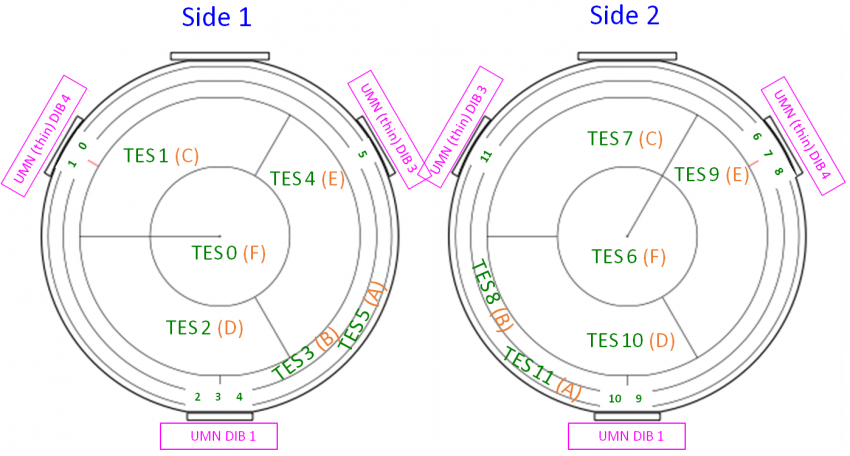 |
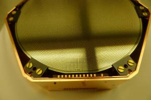 | 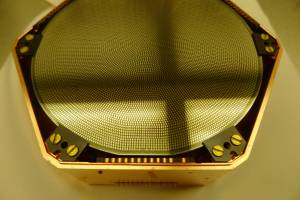 | 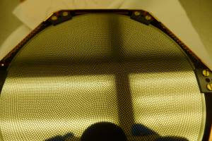 |
| Zoom to see bonds near DIB 1 | ||
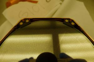 | 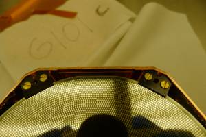 | 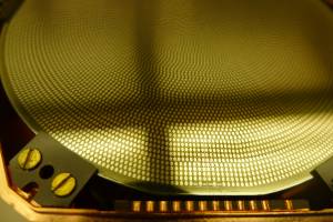 |
| Another view near DIB 1 | ||
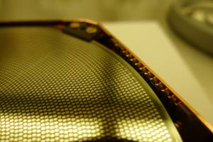 | 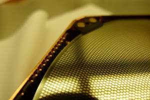 | 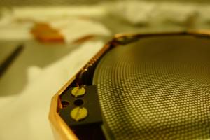 |
| Near DIB 4. Note there are only 6 gap-spanning bonds. | Bonds from DIB near DIB 3, a little blurry. | One of the other bonds near DIB 3. You can see there are letters C and E marking the bond pad locations. |
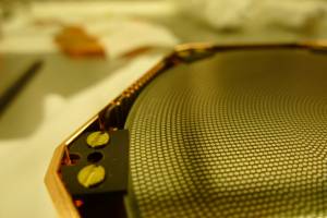 | 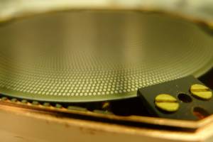 |  |
| Rotated shot of the other bonds near DIB 3, a little blurry | Better shot of the 3 bonds near DIB 3. All are from “C” to “E”. |
Lead stack idea:
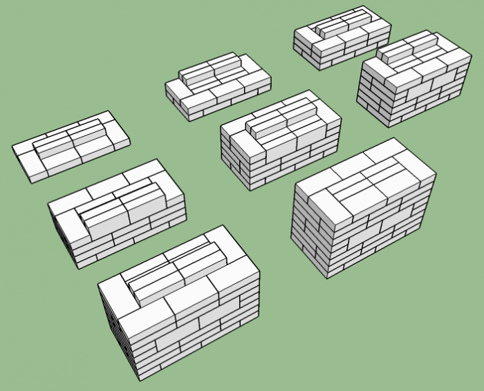
alternative (some side bricks on long edge to block more gaps)
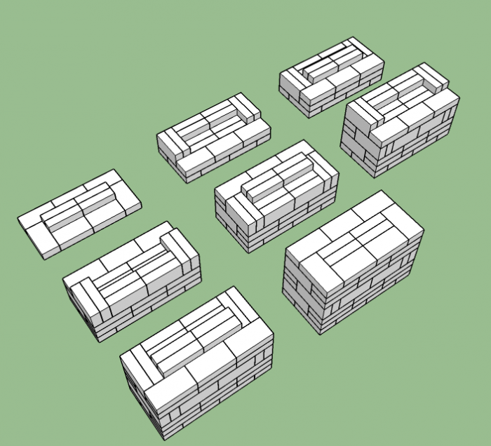
better diagram of assembly steps:
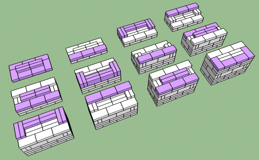
views of potential gaps for each version:
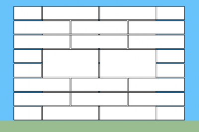 | 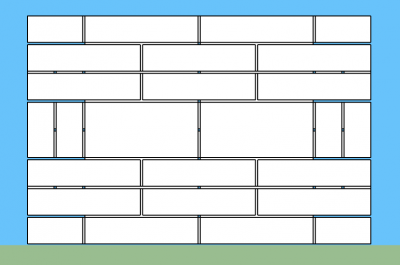 |
| 14 4-inch slit gaps on sides 7 point-like gaps along central axis | 8 4-inch slit gaps on sides 12 point-like gaps on sides 7 point-like gaps along central axis |
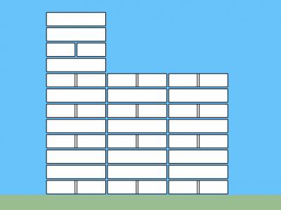 |
| original version lots of potential gaps |