UMN CDMS Wiki archive
start › cdms › k100 › run_diary › 20170706

2017/07/06 (Thursday)

Previous Day

Setup: DIB 3/4 → 3.2 MHz filters 2/3 → cable 2/3 → gender changer 3/x → DCRC33(2)/55(1)
0925 Lab = 22.1 C, 44% humidity
0935 Tower/MC/Coldplate = 28.2/30.7/179 mK, Still = 1.4 K / 0.060 mbar, G1/G2 = 126/122 mbar, 1K Pot = 1.69 K / 28 mbar. MB = 33.5%
0940 Fill LN2 cold trap bath
1100 Measure TES resistance in normal and s/c states for DIB4 channels, by measuring dIs/dIb (then Rtes = (dIb/dIs-1)*Rshunt, Rshunt = 24 mOhm)
DIB4 Rnormal/Rparasitic
Rnormal+Rpar [mOhm] Rpar [mOhm] Rnormal [mOhm]
pA 77.7 10.8 66.9
pB 66.2 9.9 56.3
pC 107.9 16.5 91.4
pD 147.2 25.3 121.9
Rpar seems to be proportional to Rnormal - why?
no reason it should
saw this in DIB3 too, not in DIB1
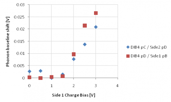
1255 Experiment with charge bias. Set DIB3 (Side1) to 4V. DIB3 charge channels show inverted pulses. Seems to push all phonon channels up higher in transition - tried adjusting one channel, DIB4pD, found it required a lower QET bias to achieve strong pulses, and the trace seemed to have wiggly low-f noise. Maybe this is a symptom of poor neutralization. Should try a bake.
1300 Try 5 minute bake with the connected DIBs, 3&4, so this is the four external LEDs, including the long-wavelength one (LED1 on DIB3). Tower heated to around 0.5 K.
1325 Start LHe transfer (MB = 27.5%, predicted level 31.1%)
1350 Tower temperature is back down to 29 mK, 45 min after bake ended
1400 The effect of charge bias on phonon channels does not seem improved after the bake. Measure shift in baseline as function of Side1 charge bias.
DCRC1 (Rev C.1) with x1 Driver Gains
1415 End LHe transfer (MB = 93.0%)
1700 Fill LN2 cold trap full.

Next Day