2016/08/12 (Friday)
| Setup: iZIP mode, DIB1/2/3 → cables → 3.2 MHz filters → DCRC55(1)/33(2)/50(3), Tower has been cooled below Al transition with mu-metal shield at standard position | |
| DCRCs powered overnight, took bg data last night. Pumping on IVC with turbo pump overnight. | |
| 0745 | Tower/MC/Coldplate = 39.5/37.3(?)/158 mK, Still = 1.32 K / 60 μbar, G1/G2 = 215/200 mbar, 1K Pot = 1.54 K / 5.0 mbar, MB = 62.7%. Boiloff rate: good. Released pressure yesterday at 27min and 52min after end of partial transfer (81%) |
| 1K Pot oscillatory, 1.52-1.56 K, 4-6 mbar, like yesterday. | |
| 0750 | Fill LN2 cold trap bath. |
| 1145 | Turn off DCRCs, in preparation for trying HV. Before that we should do electrical checkouts again, see whether anything has changed in the charge channels. Tower cools a bit after turning off DCRCs |
| 1245 | Tower/MC/Coldplate = 35.6/36.9(?)/141 mK |
| 1250 | DIB2 electrical checks: qI feedback → drain/source quite conductive, 1.43 MΩ. qI drain/source → feedback open (<1 nS). qI feedback→chassis very low, around 100 Ω; measuring this with multimeter causes spike in base temperature to 75 mK. qI drain/source → chassis <1 nS. qI chassis → drain source = 1.43 MΩ. qI bias → chassis <1 nS. This suggests a second short has developed. The first short is from the far end of the feedback resistor to chassis and is around 1.4 MΩ. The second short is on the near side of the feedback resistor and is around 0 Ω. The first short could be in the side coax or the tower or the FET card. The second short could be anywhere out to the side coax but I suspect the side coax because of the heating seen. |
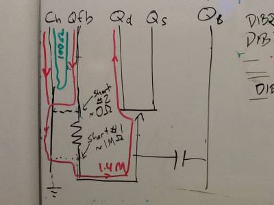
| note that there seems to be no short from the bias line to chassis, so we should be able to use the HV box. | |
| the good channel, qO, is feedback → drain/source = 20 nS, qO drain/source → feedback <1 nS, feedback/drain/source → chassis <1 nS | |
| 1400 | Set up disconnector board to break all the lines to both charge channels on DIB2. Those channels will float. |
| 1415 | Setup: HV mode, DIB1/2/3 → 3.2 MHz filters → nothing/disconnector board/remapping board → HVside2board → DCRC55(1)/50(3) |
| 1430 | On ODB, disable DCRC2, and reset phonon settings on DCRC3 to apply the settings used for the same phonon channels with the previous iZIP mapping. DCRC 3D/2C/2D are now mapped to DCRC 3B/3C/3D. |
| previous | new | |||||
|---|---|---|---|---|---|---|
| channel | lockpoint | SQ bias | QET bias | lockpoint | SQ bias | QET bias |
| DCRC3B | -3.72 | -81.2 | 107 | -4.53 | -82.6 | 130 |
| DCRC3C | -3.78 | -74.0 | 86 | -2.57 | -79.2 | 125 |
| DCRC3D | -4.53 | -82.6 | 130 | -2.76 | -93.5 | 97.7 |
| 1458 | Tower temperature has leveled off around 37.7mK, though it's still dropping slowly. |
|---|---|
| 1500 | HV tests. Watch pulses and try applying HV, monitor leakage current. |
Basic observations:
- When you increase to a new HV, leakage current is large at first then falls off quickly, stabilizing after a few minutes.
- When you back down from a higher HV, you generally get to lower leakage at first, but it increases slowly over time.
- At some point as HV is increased “breakdown noise” (jagged low-frequency stuff) appears in the phonon traces
- At some point as HV is increased pulses disappear, though they might return after time. At a higher HV pulses disappear permanently.
- When you dial HV back to zero there is backwards leakage current which decreases over a few minutes.
The table below shows measured HV and Vleakage and derived quantities for the HV tests done today. The leakages shown are the lowest seen after waiting for some time (we never waited more than about 2 minutes, sometimes shorter). As can be seen the derived leakage conductance is around 3 nS at the higher biases, meaning only 40-50% of the bias is seen at the crystal.
| HV [V] | Vleak [mV] | Vcrystal [V] | Vcrystal/HV | Ileak [nA] | Rleak [MOhm] | Gleak [nS] |
|---|---|---|---|---|---|---|
| using 40V supply | ||||||
| 1 | 1.6 | 0.3 | 0.3 | 1.76 | 168 | 5.95 |
| 4 | 5.2 | 1.71 | 0.43 | 5.72 | 299 | 3.34 |
| 10 | 10.9 | 5.2 | 0.52 | 11.99 | 434 | 2.3 |
| 20 | 21 | 10.76 | 0.54 | 23.1 | 466 | 2.15 |
| 30 | 37.1 | 13.68 | 0.46 | 40.81 | 335 | 2.98 |
| -4 | -7.5 | -0.7 | 0.18 | -8.25 | 85 | 11.79 |
| -10 | -15.3 | -3.27 | 0.33 | -16.83 | 194 | 5.15 |
| -20 | -24 | -9.44 | 0.47 | -26.4 | 358 | 2.8 |
| -30 | -38.6 | -13.02 | 0.43 | -42.46 | 307 | 3.26 |
| using 1kV supply | ||||||
| 20 | 25.8 | 8.65 | 0.43 | 28.38 | 305 | 3.28 |
| 30 | 38.5 | 13.06* | 0.44 | 42.35 | 308 | 3.24 |
| 35 | 43.8 | 15.73 | 0.45 | 48.18 | 326 | 3.06 |
| 40 | 50.5 | 17.78 | 0.44 | 55.55 | 320 | 3.12 |
| 50 | 62.6 | 22.46 | 0.45 | 68.86 | 326 | 3.07 |
| 60 | 78.5 | 25.46 | 0.42 | 86.35 | 295 | 3.39 |
| -20 | -33.3 | -5.35 | 0.27 | -36.63 | 146 | 6.85 |
| -30 | -40.4 | -12.22* | 0.41 | -44.44 | 275 | 3.64 |
| -35 | -45.8 | -14.85 | 0.42 | -50.38 | 295 | 3.39 |
| -40 | -52.5 | -16.9 | 0.42 | -57.75 | 293 | 3.42 |
The bold quantities above are the highest crystal voltages in both polarities at which some pulses could still be seen. The starred quantities are voltages at which we started to see jagged noise.
| 1635 | After experimenting with HV, switch back to iZIP mode. Set values for DCRC3 pB, pC, pD back to previous values. Unpower DCRCs 1&3, and remove HV Box. Reconnect DCRCs 1,2,3 in iZIP mode, and power up. Zap SQUIDs. |
|---|---|
| 1652 | Fill LN2 cold trap full. |
| 1715 | Pulses all look good after adjusting Driver Offsets. Commence baking overnight for 15 hours. |