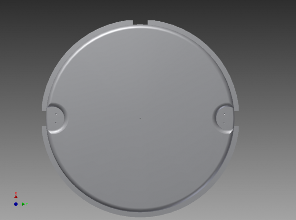
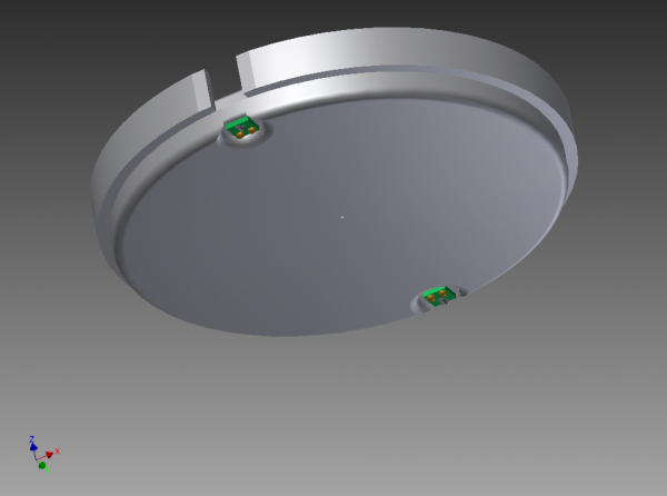
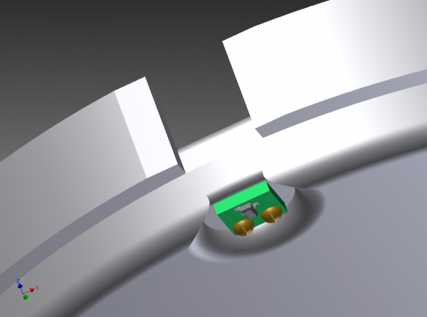
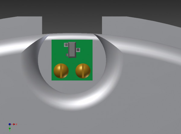
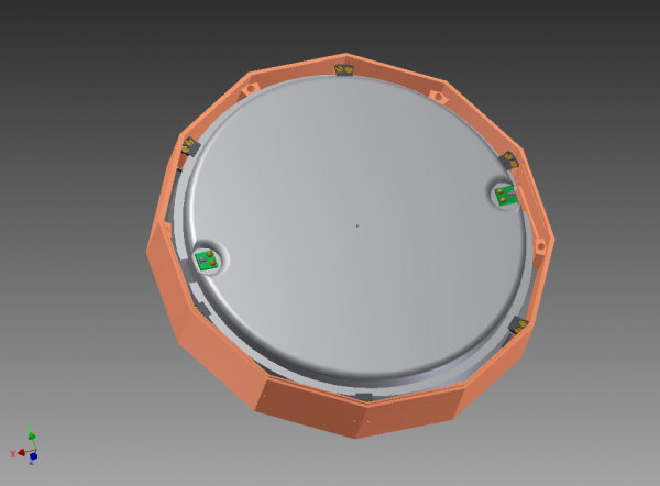
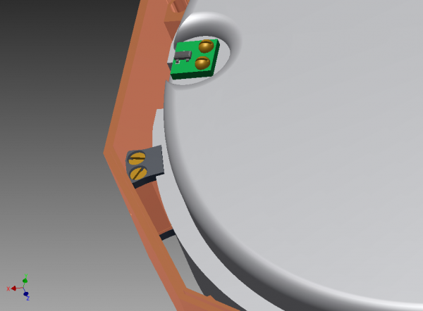
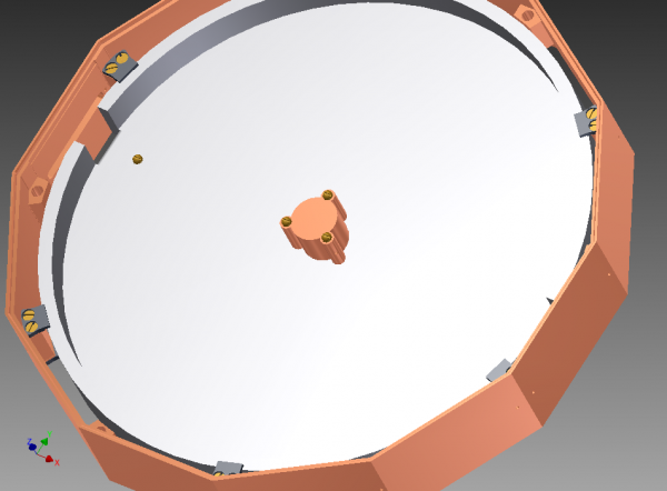
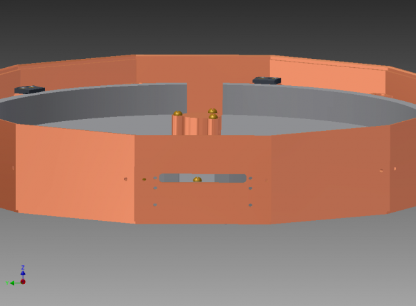
150 mm Si Detector Designs
All CAD designs can be found at /data/chocula/k100/CAD as well as on the lab's Windows Machine.
Drawings
| Part | Drawings | Status |
| HV Contract Free 1.25“ Thick |
| Electrode | 2016/03/04: 1
2016/03/21: 1 2
2016/04/01: 1 2 | Design complete, submitted to shop on 2016/04/08, and have been completed. |
| Electrode DIB | | Using standard Soudan 1” DIBs. Five Dibs were sent from Matt Cherry. |
| Electrode Top Housing | 2016/03/21: 1 2
2016/03/22: 1 2
2016/04/01: 1 2 | Design complete, submitted to shop on 2016/04/08, and have been completed. |
| Electrode Bottom Housing | 2016/03/17:1
2016/03/22: 1 2
2016/04/01: 1 2 | Design complete, submitted to shop on 2016/04/08, and have been completed. |
| Crystal Housing | 2016/03/30: 1 2
2016/04/11: 1 2 | Design complete, submitted to shop on 2016/04/08. Update to drawing made 2016/04/11 (and sent to shop). |
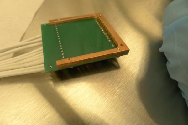
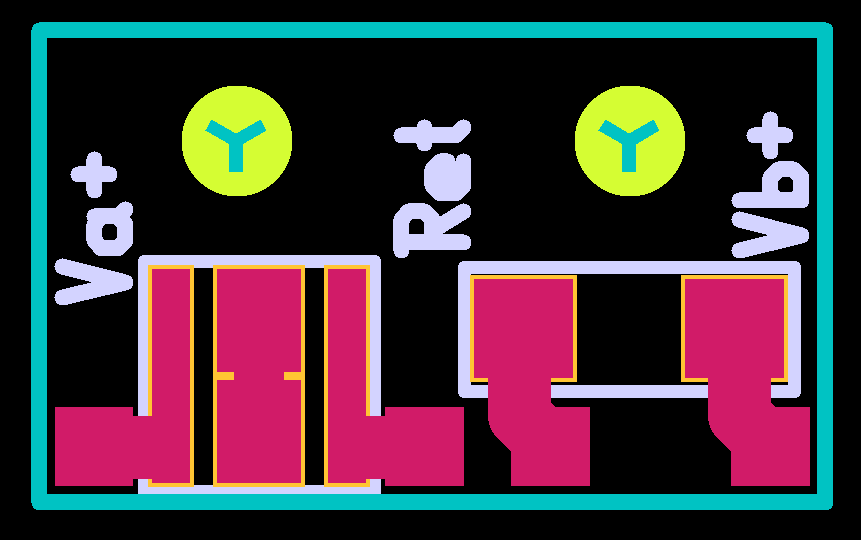
| LED PCB board | 2016/03/29:ledPCB | 6 boards successfully assembled and operational at room temp. |
| LED switchboard | | Construct from existing unused stripline diverter pcbs. One assembled for HV testing. |
| Standard Contact 1.00“ Thick |
| Detector Housing Sides | 2013/07/01: 1 2 | Design complete and fabricated. |
| Source holder (source housing + source plate) | 1 | Design complete, fits 2 small and 2 large Am sources |
| Both Crystals |
| 5, 10, 20 mil spacers | 2014/04/25: 1 | Designs complete, 72 20 mil spacers fabricated. |
| Cirlex Clamps | 2014/04/25 1 | Designs complete, 24 fabricated, and 24 submitted to shop on 2016/04/08.. |
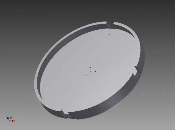
| Detector Housing Crown (top) | 2013/07/01: 1 | Design complete, one fabricated, one submitted to shop on 2016/3/23, completed on 2016/4/8. |
| Detector Housing Bottom | 2013/07/01: 1 | Design complete, one fabricated, one submitted to shop on 2016/3/23, completed on 2016/4/8. |
| Cold Hardware |
| 30 mK can | (flange) tubebottomassembled | Design complete and fabricated. |
| Adapter plate | 2016/03/17:1
2016/03/24: 1 | Design complete, submitted to shop on 2016/3/24, completed on 2016/4/8. |
Post-fabrication Assembly and Testing
2016/07/07 Assembly Update
As of July 7th 2016, all items have been completed by the workshop and are ready to be assembled and tested. The following tasks were performed in the assembly:
Standard 1” DIBs sent from Matt Cherry at Stanford, were attached to the two electrode housings.
Both electrodes were clamped into place in their housings. 20 mil spacers were used on the LED side of both electrodes. On the source/bias/readout side, 10 mil spacers were used on the readout electrode, and 20 mil spacers were used on the HV electrode.
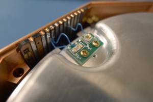
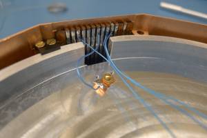
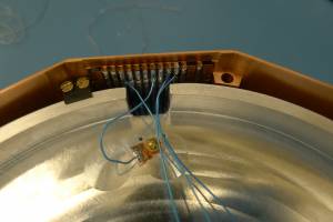
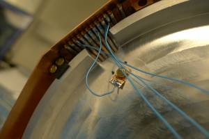
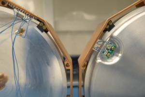
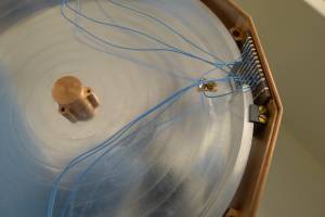
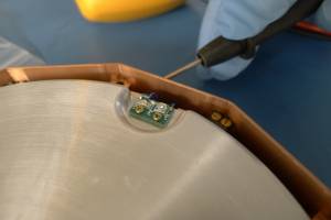
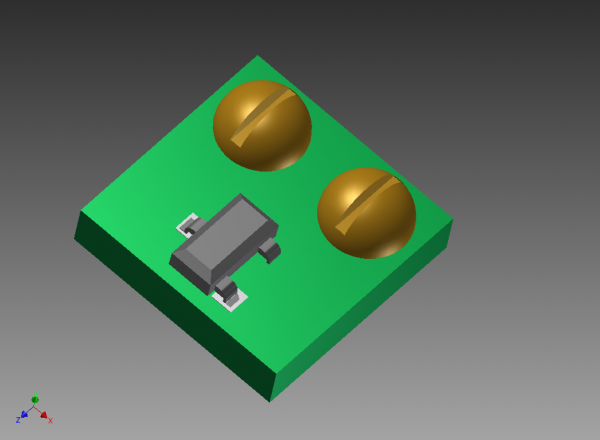
Two LED chips were attached to underside of each electrode and blue wire (type unknown) was soldered to connect DIBs and LED chips.
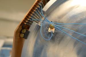
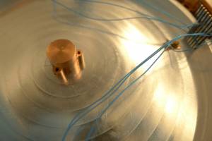
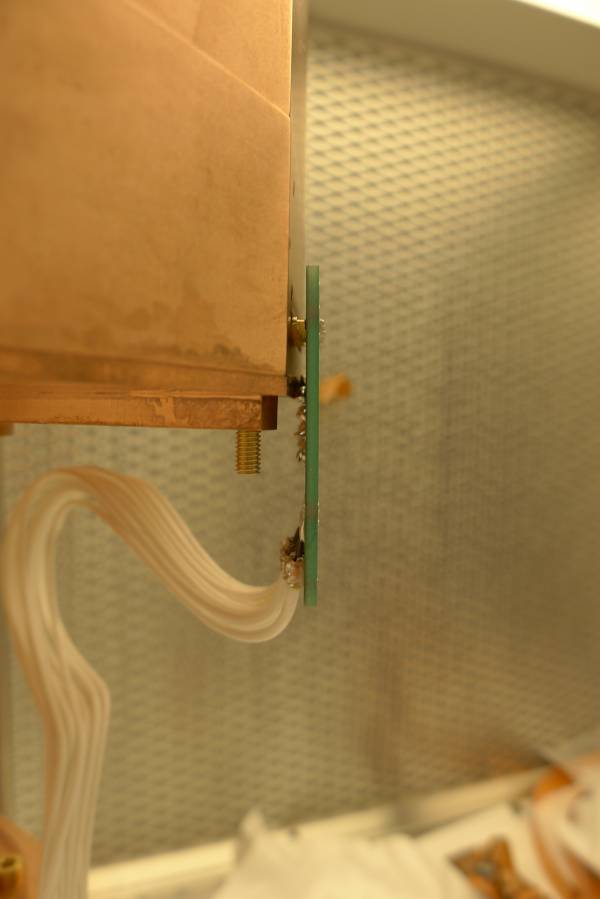
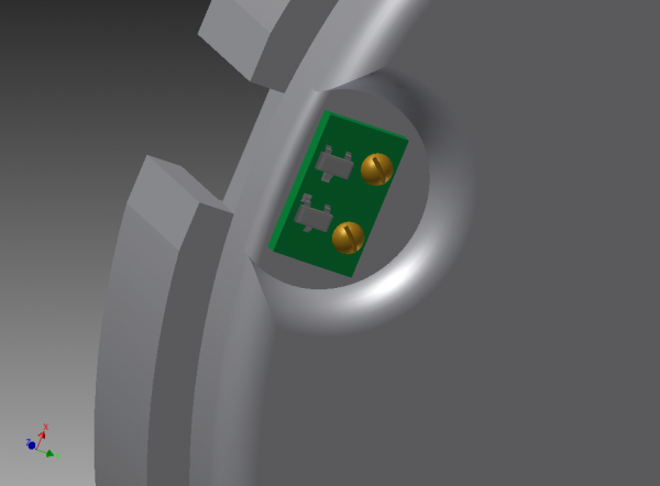
Small copper sheet was cut and folded to make two roughly 1cm x .5cm rectangles. A small hole was made in these rectangles for a 0-80 screw to pass through. A brass 0-80×5/32“ screw with a 0-80 brass nut and the one copper rectangle were screwed into the bias/readout screw hole on each electrode. The same blue wire was the soldered to the copper rectangle and the DIB.
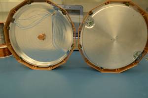
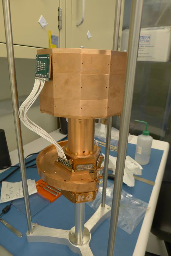
The electrodes and crystal housings were stacked with top and bottom lids and secured with threaded rods produced earlier. Stack fit well together and was secured easily with rods.
Tried to mount the stack on a tower. We found that the bottom/crown lid inner diameter was too small to fit around the spool (it should have a diameter of 2.21”, but measured 2.18“). This must be sent to the shop to be fixed.
Switched bottom/crown lid with Hassan's housing crown lid (same design). We found that this did fit around the spool, however two screw holes connecting crown to spool were mangled. This must be sent to shop to re-tap. For now, we were able to secure stack with the four remaining holes. Bad holes were marked with an 'X' in capton tape.
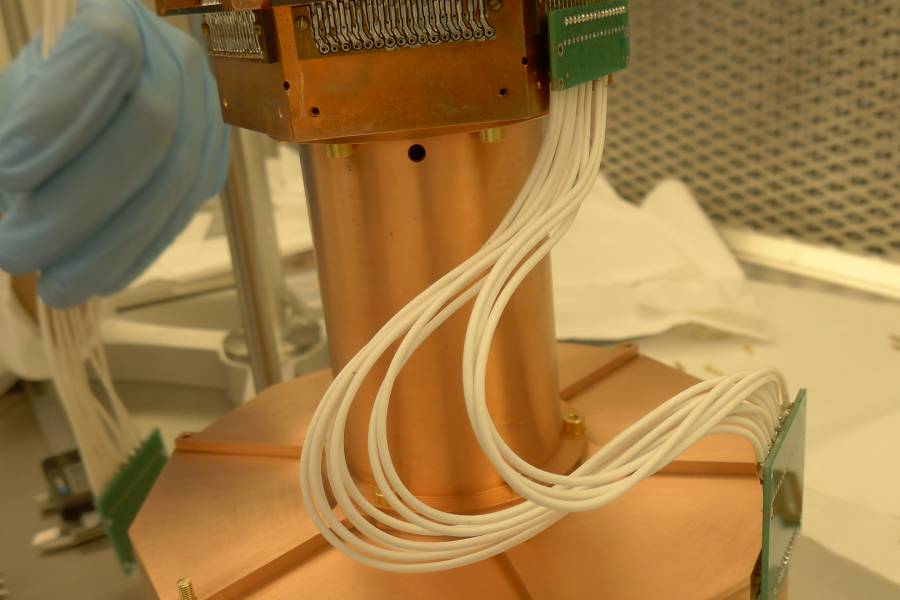
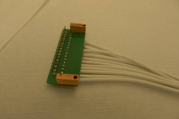
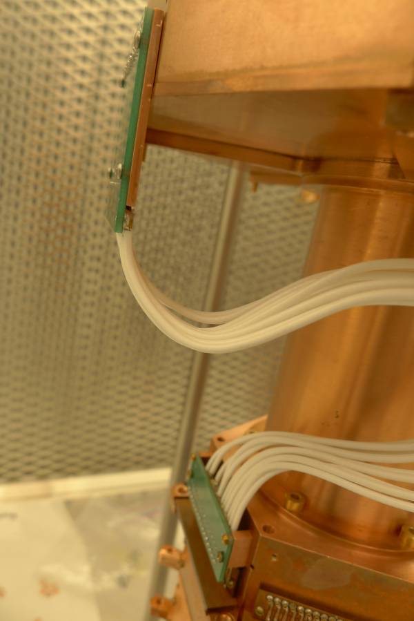
Once tower and stack were assembled, we attempted to attach flexible side coaxes. We found that the flexible side coaxes were too short to connect to the furthest electrode, since this electrode's DIB is “upside down” compared to standard designs, and requires the flexible side coax be twisted to attach. We decided to instead to move the pins to the other side of each connector, such that the flexible side coax can be connected without twisting. This must be done at a later day.
Tower was then disassembled so that electrical checks can be performed on the individual electrodes.
The electrical check determined that all LEDs are working properly and can be turned on through the DIB. Bottom electrode (used for charge readout) also showed good connection between Qouter channel and electrode, as well as <1nS between all non-LED channels and chassis. Unfortunately, top electrode (used for HV bias) showed 4.1 MΩ between electrode and chassis. After removing the Qbias screw from the electrode, we determined that this was caused by a ~MΩ between the DIB channels and chassis. We plan to replace the DIB with one of the remaining three DIBS to fix this problem.
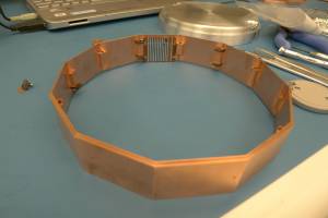
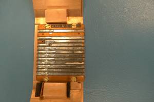
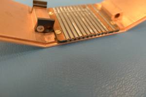
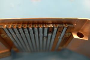
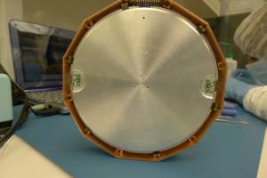
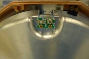
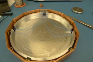
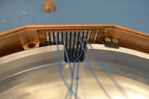
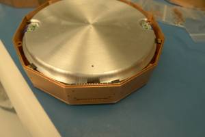
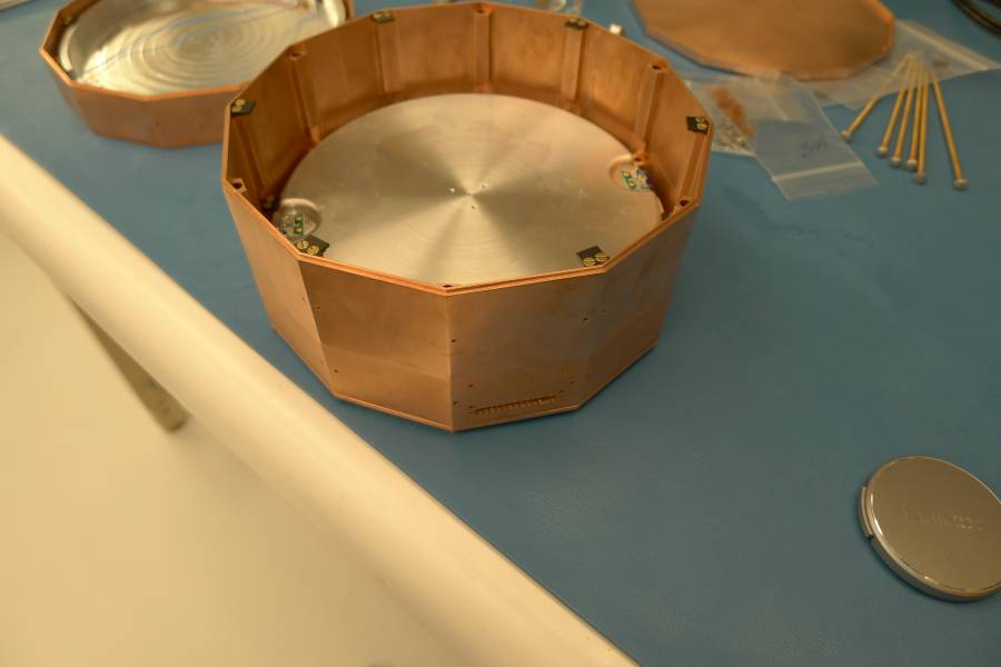
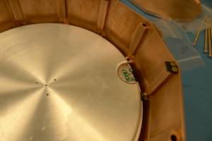
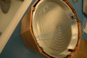
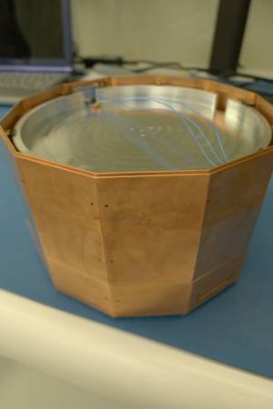
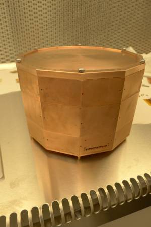
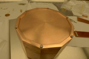
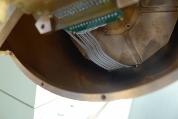
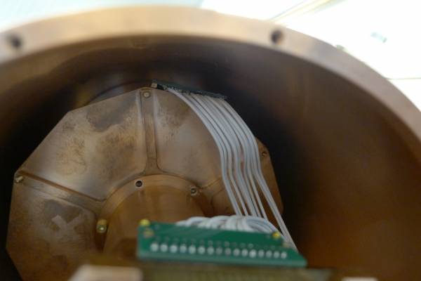
Pictures below show the electronics and assembly.
2016/07/08 Assembly Update
Today the pins on one flexible side coax were reversed (pictures and electrical check to follow), and the top electrode DIB was replaced. An electrical check on this top electrode showed all working as expected EXCEPT a ~mΩ connection between chassis and phonon D channel. It is believed this is due to some excess flux from soldering. Cleaning the DIB with isopropynol reduced the connection to ~2nS. Regardless, this channel is not used, and no other channels are connected.
2016/08/15 Crystal Mounting and Tests on Spacing Measurements
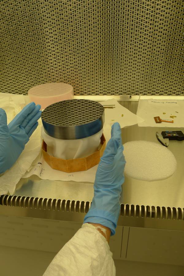
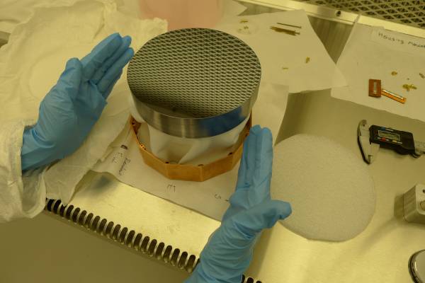
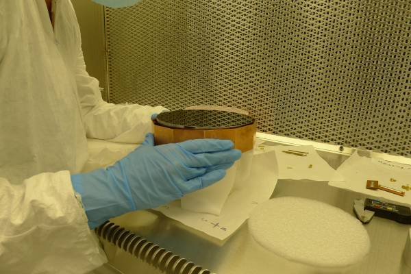
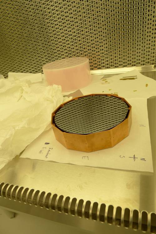
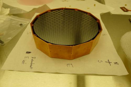
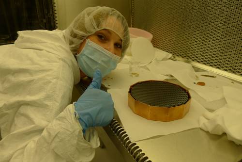
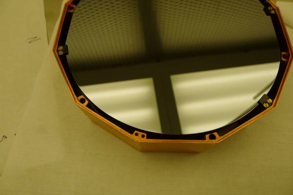
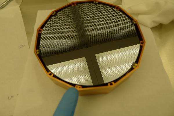
Today the crystal was mounted into its housing. To do so, 20 mil spares and clamps were put on one side of the crystal housing. A crystal stand was then assembled using a clean room plastic storage tub, some styrofoam that the crystal was packaged with, cut to be slightly smaller than the crystal, and a fabric kim wipe. The housing was set at the base of the stand, around the stand. The crystal was then set on the stand, and the housing was carefully lifted upwards. As it was lifted, the clamps on the bottom side of the housing caught on the crystal, and lifted it up from the stand. The housing and crystal were then gently set down, checking that the crystal was sitting correctly in all the clamps. Then the spacers and clamps on the second side were added, using another fabric kim wipe to guard the crystal from the screws and screw driver (along with a careful hand). Although the designs originally called for two 20 mil spacers on each side, it was determined that one 20 mil spacer was a better fit. It should also be noted that two holes in the housing were not tapped!! and thus one clamp could not be put in.
| Figures 1a and 1b: Creating the stand for crystal mounting | |
 |  |
| Figure 2: Raising the housing to catch the crystal |
 |
| Figure 3: Crystal is in housing |
 |  |  |
| Figure 4: Clamp screw holes not tapped! |
 |  |
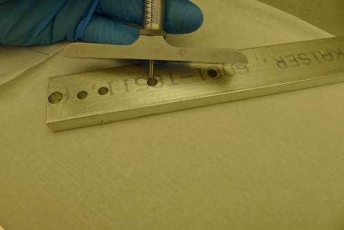
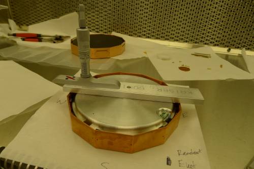
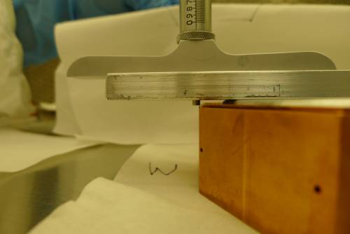
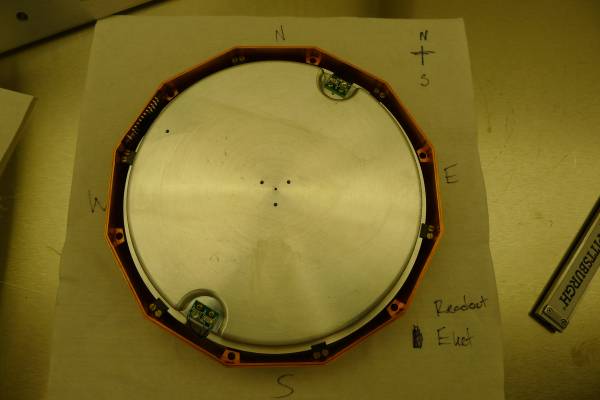
Using a aluminum bar with holes drilled near the edge, and a depth gauge micrometer, we were able to measure the distances from the electrodes and crystal to the edge of the housings. From these measurements we can calculate the gap between each electrode face and its corresponding detector side. We were originally hoping for a gap of 0.5 to 1 mm.
| Figure 5: Mechanism to measure distances |
 |  |  |
| Figure 6:NWES orientation for electrodes (DIB to NW) |
 |
| | | Bias Electrode | Crystal Side 1 | Crystal Side 2 | Readout Electrode |
| | | Measurement 1 | Measurement 2 | Mean | Measurement 1 | Measurement 2 | Mean | Measurement 1 | Measurement 2 | Mean | Measurement 1 | Measurement 2 | Mean |
| Inner Lip | North | 0.395 | 0.395 | 0.395 | 0.383 | 0.383 | 0.383 | 0.425 | 0.421 | 0.423 | 0.473 | 0.47 | 0.4715 |
| | West | 0.397 | 0.397 | 0.397 | 0.381 | 0.383 | 0.382 | 0.422 | 0.421 | 0.4215 | 0.471 | 0.474 | 0.4725 |
| | East | 0.394 | 0.394 | 0.394 | 0.381 | 0.381 | 0.381 | 0.421 | 0.421 | 0.421 | 0.473 | 0.474 | 0.4735 |
| | South | 0.394 | 0.393 | 0.3935 | 0.381 | 0.383 | 0.382 | 0.423 | 0.421 | 0.422 | 0.474 | 0.473 | 0.4735 |
| Outer Lip | North | 0.445 | 0.445 | 0.445 | 0.431 | 0.431 | 0.431 | 0.386 | 0.382 | 0.384 | 0.431 | 0.43 | 0.4305 |
| | West | 0.447 | 0.447 | 0.447 | 0.431 | 0.431 | 0.431 | 0.386 | 0.382 | 0.384 | 0.431 | 0.43 | 0.4305 |
| | East | 0.445 | 0.445 | 0.445 | 0.43 | 0.43 | 0.43 | 0.382 | 0.382 | 0.382 | 0.432 | 0.432 | 0.432 |
| | South | 0.444 | 0.444 | 0.444 | 0.431 | 0.432 | 0.4315 | 0.383 | 0.381 | 0.382 | 0.433 | 0.433 | 0.433 |
| Electrode/Crystal | North | 0.382 | 0.384 | 0.383 | 0.488 | 0.487 | 0.4875 | 0.464 | 0.464 | 0.464 | 0.383 | 0.383 | 0.383 |
| | West | 0.382 | 0.382 | 0.382 | 0.487 | 0.485 | 0.486 | 0.464 | 0.464 | 0.464 | 0.382 | 0.382 | 0.382 |
| | East | 0.382 | 0.383 | 0.3825 | 0.49 | 0.489 | 0.4895 | 0.466 | 0.466 | 0.466 | 0.382 | 0.383 | 0.3825 |
| | South | 0.382 | 0.382 | 0.382 | 0.488 | 0.488 | 0.488 | 0.465 | 0.465 | 0.465 | 0.383 | 0.383 | 0.383 |
| Outer-Inner | N | | | 0.05 | | | 0.048 | | | -0.039 | | | -0.041 |
| | S | | | 0.05 | | | 0.049 | | | -0.0375 | | | -0.042 |
| | E | | | 0.051 | | | 0.049 | | | -0.039 | | | -0.0415 |
| | W | | | 0.0505 | | | 0.0495 | | | -0.04 | | | -0.0405 |
| Outer-Device | N | | | 0.062 | | | -0.0565 | | | -0.08 | | | 0.0475 |
| | S | | | 0.065 | | | -0.055 | | | -0.08 | | | 0.0485 |
| | E | | | 0.0625 | | | -0.0595 | | | -0.084 | | | 0.0495 |
| | W | | | 0.062 | | | -0.0565 | | | -0.083 | | | 0.05 |
| Gap | Inches | mm |
| | Side 1/Readout | Side 2/Bias | Side 1/Readout | Side 2/Bias |
| N | -0.009 | -0.018 | 0.2286 | 0.4572 |
| S | -0.0065 | -0.015 | 0.1651 | 0.381 |
| E | -0.01 | -0.0215 | 0.254 | 0.5461 |
| W | -0.0065 | -0.021 | 0.1651 | 0.5334 |
Due to fears of metal contracting at cold temperatures, additional 5 mil spacers were added to both sides of the detector. New measurements were then made of the detector distances, shown below:
| | | Crystal Side 1 | Crystal Side 2 |
| | | Measurement 1 | Measurement 1 |
| Inner Lip | North | 0.381 | 0.421 |
| | West | 0.381 | 0.421 |
| | East | 0.382 | 0.422 |
| | South | 0.382 | 0.422 |
| Outer Lip | North | 0.431 | 0.382 |
| | West | 0.431 | 0.383 |
| | East | 0.432 | 0.382 |
| | South | 0.431 | 0.382 |
| Electrode/Crystal | North | 0.491 | 0.462 |
| | West | 0.490 | 0.460 |
| | East | 0.492 | 0.461 |
| | South | 0.493 | 0.461 |
| | | Bias Electrode | Crystal Side 1 | Crystal Side 2 | Readout Electrode |
| | | Measurement 1 | Measurement 2 | Mean | Measurement 1 | Measurement 2 | Mean | Measurement 1 | Measurement 2 | Mean | Measurement 1 | Measurement 2 | Mean |
| Outer-Inner | N | | | 0.05 | | | 0.050 | | | -0.039 | | | -0.041 |
| | S | | | 0.05 | | | 0.050 | | | -0.038 | | | -0.042 |
| | E | | | 0.051 | | | 0.050 | | | -0.040 | | | -0.0415 |
| | W | | | 0.0505 | | | 0.049 | | | -0.04 | | | -0.0405 |
| Outer-Device | N | | | 0.062 | | | -0.06 | | | -0.08 | | | 0.0475 |
| | S | | | 0.065 | | | -0.059 | | | -0.077 | | | 0.0485 |
| | E | | | 0.0625 | | | -0.060 | | | -0.079 | | | 0.0495 |
| | W | | | 0.062 | | | -0.062 | | | -0.079 | | | 0.05 |
| Gap | Inches | mm |
| | Side 1/Readout | Side 2/Bias | Side 1/Readout | Side 2/Bias |
| N | -0.0125 | -0.0180 | 0.3175 | 0.4572 |
| S | -0.0105 | -0.0120 | 0.2667 | 0.3048 |
| E | -0.0105 | -0.0165 | 0.2667 | 0.4191 |
| W | -0.0120 | -0.0170 | 0.3048 | 0.4318 |
2016/08/17 Stack Assembly
2016/08/18 Stack Assembly
| Detector | 150mm Si Contact Free | DIB | Bias | |
| side coax | Flex | date/who: | 2016-08-18 | AK NM |
| tower | Tower 1 | Face | 2 | |
| +lead | - lead | signal | typical | measured |
| 3 | chassis | UV LED1 Rforward | 50kΩ | 60kΩ |
| 3 | chassis | UV LED1 Vforward | open | open |
| chassis | 3 | UV LED1 Vreverse | 0.78V | 0.786V |
| chassis | 3 | UV LED1 Rreverse | 50kΩ | 52kΩ |
| 5 | chassis | UV LED2 Rforward | 50kΩ | 78kΩ |
| 5 | chassis | UV LED2 Vforward | open | open |
| chassis | 5 | UV LED2 Vreverse | 0.78V | 0.78V |
| chassis | 5 | UV LED2 Rreverse | 50kΩ | 78kΩ |
| 7 | chassis | HV QBias | <1nS | <1nS |
| 9 | chassis | IR LED1 Rforward | 0.78MΩ | 0.798MΩ |
| 9 | chassis | IR LED1 Vforward | 1.06V | 1.091V |
| chassis | 9 | IR LED1 Vreverse | open | open |
| chassis | 9 | IR LED1 Rreverse | <1nS | <1nS |
| 10 | chassis | IR LED2 Rforward | 0.78MΩ | 0.798MΩ |
| 10 | chassis | IR LED2 Vforward | 1.06V | 1.091V |
| chassis | 10 | IR LED2 Vreverse | open | open |
| chassis | 10 | IR LED2 Rreverse | <1nS | 12MΩ |
| All pins (except LED) | chassis | | <1nS | <1nS |
| Detector | 150mm Si Contact Free | DIB | Readout | |
| side coax | Flex | date/who: | 2016-08-18 | AK NM |
| tower | Tower 1 | Face | 5 | |
| +lead | - lead | signal | typical | measured |
| 3 | chassis | UV LED1 Rforward | 50kΩ | 56kΩ |
| 3 | chassis | UV LED1 Vforward | open | open |
| chassis | 3 | UV LED1 Vreverse | 0.78V | 0.78V |
| chassis | 3 | UV LED1 Rreverse | 50kΩ | 52kΩ |
| 5 | chassis | UV LED2 Rforward | 50kΩ | 36.6kΩ |
| 5 | chassis | UV LED2 Vforward | open | open |
| chassis | 5 | UV LED2 Vreverse | 0.78V | 0.781V |
| chassis | 5 | UV LED2 Rreverse | 50kΩ | 37.2kΩ |
| 9 | chassis | IR LED1 Rforward | 0.78MΩ | 0.801MΩ |
| 9 | chassis | IR LED1 Vforward | 1.06V | 1.09V |
| chassis | 9 | IR LED1 Vreverse | open | open |
| chassis | 9 | IR LED1 Rreverse | <1nS | <1nS |
| 10 | chassis | IR LED2 Rforward | 0.78MΩ | 0.78MΩ |
| 10 | chassis | IR LED2 Vforward | 1.06V | 1.09V |
| chassis | 10 | IR LED2 Vreverse | open | open |
| chassis | 10 | IR LED2 Rreverse | <1nS | <1nS |
| 12 | 11 | Qo C coupling | <1nS | <1nS |
| 12 | 13 | Qo Rfeedback | 24 to 26 nS | 25nS |
| All pins (except LED) | chassis | | <1nS | 1nS |
HV Fridge and Hardware Testing
Dan's Flexible Side Coax
On 2016/03/03 current leakage tests were performed on one of Dan's three flexible side coaxes. Before tests were performed, a quick resistance test was conducted to ensure resistances matched what was inspected. Results shown in table below. It was also noted that flexible side coaxes only have wires connecting Charge pins. Although wires connecting phonon pins will not be necessary, we will likely need wires for the LED pins, since those will likely be connected to the electrode DIB.
| Resistance Check |
| + lead pin | Detector Side | Tower Side |
| - pin (tower side) | 12 (Qi) | 11 (Qo) | 16 (Qi Feedback) | 15 (Qi Gate) | 14 (Qi Bias) | 13 (Qi Feedback) | 12 (Qi Gate) | 11 (Qi Bias) |
| 16 (Qi Feedback) | OL | OL | | 39.9 MΩ | OL | OL | OL | OL |
| 15 (Qi Gate) | OL | OL | 39.9 MΩ | | OL | OL | OL | OL |
| 14 (Qi Bias) | 40 MΩ | OL | OL | OL | | OL | OL | OL |
| 13 (Qi Feedback) | OL | OL | OL | OL | OL | | 39.9 MΩ | OL |
| 12 (Qi Gate) | OL | OL | OL | OL | OL | 39.9 MΩ | | OL |
| 11 (Qi Bias) | OL | 40 MΩ | OL | OL | OL | OL | OL | |
These result match was was expected, given the side coax schematic. It was decided that leakage current was to be tested by supplying positive and negative voltages to the Qi Bias and Qo bias pins on the tower side (pins 11 and 14, respectively). Before the negative lead connected to the pin, it would pass through an ammeter to measure any leakage current that might occur. A voltmeter would be hooked up to the leads of the high voltage supply to get a more accurate voltage reading. The test was performed with both orientations of leads to pins. Results shown in table below, but in general no leakage current was seen.
| Voltage | Leakage Current ( + lead to Qi bias, - lead to Qo bias) | Leakage Current ( + lead to Qo bias, - lead to Qi bias) |
| -0.001 V (V supply off, + lead to Qi)/-0.012 (V supply off, + lead to Qo) | .01 mA | .01 mA |
| -0.105 V | < 0.01 mA | < 0.01 mA |
| 82 V | < 0.01 mA | < 0.01 mA |
| 185.4 V | < 0.01 mA | < 0.01 mA |
| 289.2 V | < 0.01 mA | < 0.01 mA |
| 392.6 V | < 0.01 mA | < 0.01 mA |
| 496.1 V | < 0.01 mA | < 0.01 mA |
| 599.4 V | < 0.01 mA | < 0.01 mA |
| 703 V | < 0.01 mA | < 0.01 mA |
| 806 V | < 0.01 mA | < 0.01 mA |
| 910 V | < 0.01 mA | < 0.01 mA |
| 1039 V | < 0.01 mA | < 0.01 mA |
2016/05/31 Update
LED 1 and 2 wires were added to two of the flexible side coaxes, using the same wire type used for charge. As following the schematic, these wires connect pins 9 (LED 1) on both sides of the coax, and pins 10 (LED) on both sides of the coax. After soldering, electrical checks were performed to ensure no shorts between pins or to ground.
Striplines
Tests from 2016/03/24 (Thursday):
| 1525 | Testing resistance of broken stripline in clean room. Using Ohm meter, checked resistance between cold-end pins and stripline ground plane. All > 1 GOhm. Also checked a subset of adjacent pins and found R_ij > 1 GOhm. |
| 1541 | Repeating pin-pin measurements using MegOhmmeter. At TΩ scale, body movements near setup cause momentary resistance changes. |
| +lead | - lead | Resistance | |
| 1 | 14 | > 1 TΩ | Adjacent on stripline. |
| 1 | 15 | > 1 TΩ | |
| 13 | 15 | > 1 TΩ | |
| 1 | GND pin | > 1 TΩ | |
LEDs
| 1 June 2016 | With 1kΩ resistor in series, measured I-V curves of LEDs at room temperature. In the graphs shown, “pulsed” means each measurement was made by setting the bias voltage and then connecting the circuit only for a fraction of a second to measure the current. |
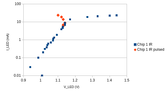
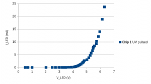
Tower
Control and Readout wiring
Proposed wiring scheme (16 June 2016)
| TOP | | BOTTOM |
| DIB line | connected to | | DIB line | connected to |
| PA ret | | | PA ret | |
| PA | | | PA | |
| PB ret | UV LED 1 | | PB ret | UV LED 1 |
| PB | | | PB | |
| PC ret | UV LED 2 | | PC ret | UV LED 2 |
| PC | | | PC | |
| PD ret | HV Qbias | | PD ret | |
| PD | | | PD | |
| LED1 | IR LED 1 | | LED1 | IR LED 1 |
| LED2 | IR LED 2 | | LED2 | IR LED 2 |
| QO | | | QO | Q readout |
| QI | | | QI | |
| 13 Sept 2016 | Due to a lack of flexible side coax cable, the HV Qbias was wired to PD returns even though the HV box must bias it via the PA returns. This is being remedied with the same switchable warm end diverter board being used to change between LEDs. |
Design Details
LED
LED choice: IR25-21C/TR8
UV LED choice: E305SL
| | IR25-21C/TR8 Stats | E305SL Stats |
| Maker | Everlight | International Light Technologies |
| Wavelength | 940 nm @ 20 mA | 310 +/5 nm @ 20mA |
| Material | GaAlAs | Si Lens |
| Chip Size | 320 x 160 x 110 um | 345 x 345 x ~190 um |
| Emission Angle | 160 ° | 120 ° |
| Operating Temperature | -25 to 85 °C | -20 to 45 °C |
| Spectral Halfwidth/bandwidth | 45 nm @ 20 mA | 10 nm @ 20mA |
| Output Power | | min: .5 mW, typ: 1 mW @ 20 mA |
| Forward Voltage | max: 1.5 V, typ: 1.2 V @ 20 mA | max: 4 V, typ: 5.5 V @ 20 mA |
| Unit Price | $0.50 | $29.99 (must buy 10) | |
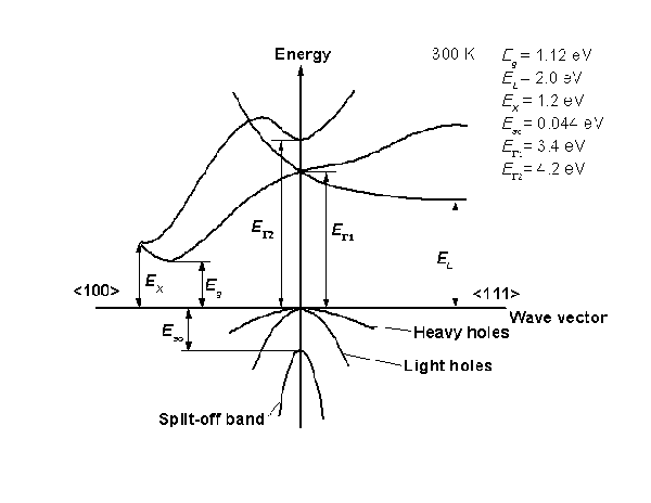
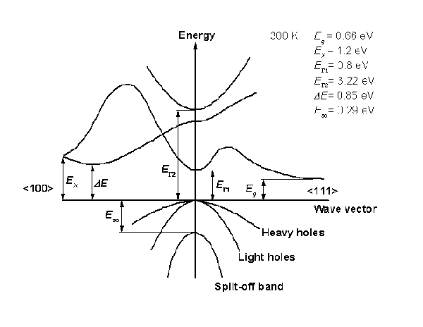
As the table shows, the traditional LED is an IR LED with a 940 nm (1.32 eV) and provides enough energy to excite to the indirect Si band gap or the Ge direct bandgap. The new UV LED is 310 nm (4.0 eV) and would provide enough energy to excite to the Si direct band gap.
| Si Bandgap | Ge Bandgap |
 |  |
HV electrode design