−Table of Contents
100 mm Contact Free Detector
This is a landing page for the designs of a 100 mm contact free detector. The first plan is to use an existing 100mm CDMS HV detector and an external electrode.
Electrode Design
G101C (HV2) Measurements
Measurements of the G101C housing lip and detector position were made using both a depth micrometer and calipers. The measurements are in the figure below.
| G101C measurements | ||||
|---|---|---|---|---|
| Diagram | Length | Micrometer | Calipers | Average |
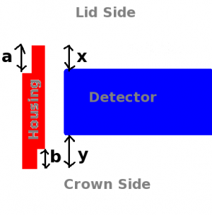 | a | 0.049“ | 0.043” | 0.046“ |
| x | 0.0525” | 0.06“ | 0.0563” | |
| b | 0.0505“ | 0.049” | 0.0498“ | |
| y | 0.091” | 0.094“ | 0.0925” | |
Electrode dimensions
- The electrode has been designed to produces a 0.7 mm (0.028“) gap between it and the detector surface
- The thickness of the electrode base is designed for a total of 0.080” of spacers, which allows for ±0.040“ adjustment in vertical position
100mm Contact Free Electrode design drawing
Electric Field Simulation
One question is to whether the TESs patterned on the bias side of the detector need to be removed. It is thought that this is not required and, in fact, their presence may help maintain a uniform electric field in the crystal. A basic simulation of these configurations were performed in COMSOL.
The model used is on galba at /scratch/mast/comsol/cf_detector.mph
Fig. 1 shows a 3D perspective of the model and an example 2D potential map. It includes a 100 mm x 33.3 mm Si detector with 0.1 mm planar electrodes on either face and a contact free electrode above the detector separated by a small gap. COMSOL calculates the resulting electric fields when 100V is applied to the contact free electrode and the housing and bottom electrodes are held at ground. In some simulations, the upper planar electrode is removed. When present, its voltage is allowed to float.
| Fig. 1 : Example of Comsol model | |
|---|---|
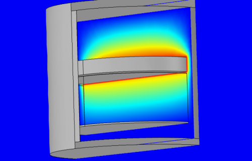 | 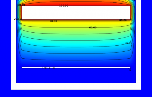 |
Fig. 2 shows two plots of voltage as a function of z (vertical) position at a variety of radii. The contact free electrode is at z=-1 mm and the crystal top is at z=0 mm. The bottom crystal electrode is at 33.3 mm. The three radii are at r=0 mm (center), r=25 mm, and r=50 mm(edge). In all figures shown, the vacuum gap causes the largest loss of applied potential as expected.
The left plot of Fig. 2 shows the results of removing the top crystal electrode. At high radius, there is a greater voltage drop across the vacuum gap, then the voltage sags a bit in z. The right plot shows the results of having a single floating planar electrode on the top of the crystal. The high radius voltage still sags, but the drop across the vacuum is uniform. In this second configuration, the field shape is likely nearly identical to that experienced when using the top electrode itself to bias.
| Fig. 2 : Voltage vs z | |
|---|---|
 |  |
Fig. 3 shows the results of using more realistic detector electrode geometries. The plot in Fig 2. above assumed a single electrode of r=50mm. In practice, the phonon mask does not reach to the full crystal radius of 50 mm, instead stopping around r=48.1 mm to leave space for clamps. the left side of Fig. 3 shows the results with a single floating electrode of r=48.1 mm. The vacuum drop at high radius is seen to be worse than the 50mm electrode, but better than a bare crystal. The right side of Fig 3. shows the voltage patterns when there is a single outer electrode with the dimensions of phonon channel A and a single inner electrode with a radius of channel B (i.e. channels B-F all connected together) and all channels floating. In these plots, there is no discernible difference between the two scenarios presented in Fig. 3.
| Fig. 3 More realistic electrodes | |
|---|---|
 |  |
These simulations indicates that
- Leaving the TESs on the crystal bias side but letting them float with a contact free electrode will give a more uniform electric field than if they were completely removed
- Disconnecting the channel segments radially will have a small impact on the overall field shape
- Because there is not expected to be significant azimuthal electric field, disconnecting the A or B channel segments should not distort the field either